Download
1 / 20
200 likes | 355 Views
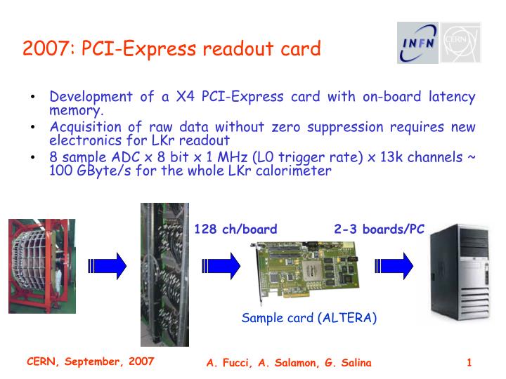
2007: PCI-Express readout card. Development of a X4 PCI-Express card with on-board latency memory. Acquisition of raw data without zero suppression requires new electronics for LKr readout 8 sample ADC x 8 bit x 1 MHz (L0 trigger rate) x 13k channels ~ 100 GByte/s for the whole LKr calorimeter.

E N D
2007: PCI-Express readout card • Development of a X4 PCI-Express card with on-board latency memory. • Acquisition of raw data without zero suppression requires new electronics for LKr readout • 8 sample ADC x 8 bit x 1 MHz (L0 trigger rate) x 13k channels ~ 100 GByte/s for the whole LKr calorimeter 128 ch/board 2-3 boards/PC Sample card (ALTERA)
Printed Circuit Board 12 layer: 6 routing layers and 6 gnd/power layers conn. EEPROM JTAG DDR2 mezzanine FPGA foro PCI-E lines linear switching
2.5 GBit/s lines FPGA PCI-E x4 Connector 4 x 2.5 Gbit/s transmitters, 4 x 2.5 Gbit/s receivers, 1 x 125 MHz clock
12 different power supplies:6 switching + 6 linear regulators Power planes
Routing 0-1 layer DDR2 FPGA
Routing 2-3 layer DDR2 FPGA
Routing 4-5 layer DDR2 FPGA
Routing 6 layer DDR2 FPGA
Time schedule • PCB layout: 15 working days • PCB manufacturing: 10 working days • PCB assembly: 15 working days Schematic is finished We are finishing PCB layout 8 weeks firt tests: half of november
2008: LKr trigger electronics RD LKr trigger electronics is 10 years old and must be redesigned for the 1 MHz readout • 216 Fastbus modules • 32 data concentrators • 16 processors During 2008 we are planning to design a VME (9U) based trigger system Flash ADC, FPGA, high speed links
LKr trigger electronics requirements • Digitization • Halo expansion • Time, energy and position extraction • Trigger algorithm execution
8 channels block DDR2 latency memory DDR2 interface ADC 0: 12 b @ 40 MHz Readout path: 16 b @ 80 MHz ADC 7: 12 b @ 40 MHz Trigger path: (4 ch digital sum) 16 b @ 80 MHz Working assumption: front-end mezzanines to perform digitization, digital sum and storage during the latency period. We found some low-cost, low-power components for the ADC, latency memory and FPGA and also a possible implementation.
8 1 8 1 4 1 1 4 1st layer Conc board: halo expansionfine timingtrig candidat generreadout comm propag 3rd layer Conc board: trig candidat selectiontrig generationreadout comm generat FE board: digitizationdigital sumL1 latency memoryreadout to PC 2nd layer Conc board: trig candidat selectionreadout comm prop 216 x 54 x 7 x 1 x FE board Conc board Conc board Conc board 64 ch 256 ch 2048 ch 13k ch Front-end mezzanines Halo expansion and fine timing in the first layer concentrator board! Starting from the 1st layer all Conc Boards work on energy-position-time cluster lists! Conc board 256 ch 1st layer Conc board
FE Board FE Board FE Board FE Board FE Board FE Board FE Board FE Board FE Board FE Board FE Board FE Board FE Board FE Board FE Board FE Board VME master Conc Board Conc Board Conc Board Conc Board Crate: front side Communication between FE Board and Concentrator Board on the backplane Communication between Concentrator Boards (for halo expansion and between different Concentrator Boards) on the front side
Left FE Board – 9U x 400mm - 64 channels – 216 boards CH 0 CH 1 1 trigger link 1 GByte/s 1 service link 200+200 MByte/s CH 63 1 readout link To L1 PCs 1 GByte/s
1st layer Concentrator Board – 9U x 400mm - 256 channels – 54 boards halo exp link (UP) 500+500 MByte/s 2 trigger links 1 GByte/s each halo exp link (LEFT) 500+500 MByte/s 1 service link 200+200 MByte/s halo exp link (RIGHT) 500+500 MByte/s 2 trigger links 1 GByte/s each halo exp link (DOWN) 500+500 MByte/s 1 service link 200+200 MByte/s 1st-2nd layer concentrator link 200+200 MByte/s
2nd layer Concentrator Board – 9U x 400mm - 2048 channels – 7 boards 1st-2nd layer concentrator link 0 200+200 MByte/s 1st-2nd layer concentrator link 1 200+200 MByte/s 1st-2nd layer concentrator link 7 200+200 MByte/s 2nd-3rd layer concentrator link 200+200 MByte/s
Components • ADC: Maxim MAX1436B octal 12 bit 40 MSps low power (100 mW per channel) ADC: 33 Euro (Maxim) • FPGA: Altera EP2C5F256C7 16 Euro (EBV) • DDR2: Samsung K4T51163QE 512 Mbit (32 Mword x 16) 15 Euro (EBV) • Link 500+500 MB/s o 1 GB/s: National Semiconductors DS90CR485 -DS90CR486: 27 Euro/chip • Link 200+200 MB/s: Texas Instruments TLK2501: 20 Euro/chip
3rd layer Concentrator Board – 9U x 400mm – 13k channels - 1 board 2nd-3rd layer concentrator link 0 200+200 MByte/s 2nd-3rd layer concentrator link 1 200+200 MByte/s 2nd-3rd layer concentrator link 7 200+200 MByte/s