Download
1 / 23
230 likes | 414 Views
Unit 8 Combinational Circuit Design and Simulation Using Gates. Ku-Yaw Chang canseco@mail.dyu.edu.tw Assistant Professor, Department of Computer Science and Information Engineering Da-Yeh University. Contents. 8.1 Review of Combinational Circuit Design

E N D
Unit 8Combinational Circuit Design and Simulation Using Gates Ku-Yaw Chang canseco@mail.dyu.edu.tw Assistant Professor, Department of Computer Science and Information Engineering Da-Yeh University
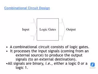
Contents 8.1 Review of Combinational Circuit Design 8.2 Design Circuits with Limited Gate Fan-In 8.3 Gate Delays and Timing Diagrams 8.4 Hazards in Combinational Logic 8.5 Simulation and Testing of Logic Circuits Fundamentals of Logic Design
Propagation Delay In nanoseconds Fundamentals of Logic Design
Timing Diagram • Frequently used in the analysis of sequential circuits Fundamentals of Logic Design
Timing Diagram With Delay Fundamentals of Logic Design
Contents 8.1 Review of Combinational Circuit Design 8.2 Design Circuits with Limited Gate Fan-In 8.3 Gate Delays and Timing Diagrams 8.4 Hazards in Combinational Logic 8.5 Simulation and Testing of Logic Circuits Fundamentals of Logic Design
Hazards • When the input to a combinational circuit changes, unwanted switching transients may appear in the output. • Different paths • Different propagation delays Fundamentals of Logic Design
Types of Hazards Fundamentals of Logic Design
A Static 1-hazard • A = C = 1 • F = AB’ + BC = B + B’ = 1 • F should remain a constant 1 when B changes from 1 to 0. • Assumption • A propagation delayof 10 ns Fundamentals of Logic Design
A Static 1-hazard Fundamentals of Logic Design
Hazard Detection • Write down the sum-of-products expression for the circuit. • Plot each term on the map and loop it. • If any two adjacent 1’s are not covered by the same loop, a 1-hazard exists for the transition between the two 1’s. Fundamentals of Logic Design
Hazard Removal • Add a loop on the Karnaugh map • Corresponding gate Fundamentals of Logic Design
0-hazards • Product of sums • F = (A+C)(A’+D’)(B’+C’+D) • Four pairs of adjacent 0’s that are not covered by a common loop • Each corresponds to a 0-hazard Fundamentals of Logic Design
0-hazards =0 =0 =1 Fundamentals of Logic Design
Removing Hazards • Eliminate the 0-hazards • F=(A+C)(A’+D’)(B’+C’+D)(C+D’)(A+B’+D)(A’+B’+C’) Fundamentals of Logic Design
Contents 8.1 Review of Combinational Circuit Design 8.2 Design Circuits with Limited Gate Fan-In 8.3 Gate Delays and Timing Diagrams 8.4 Hazards in Combinational Logic 8.5 Simulation and Testing of Logic Circuits Fundamentals of Logic Design
Verification • Building a circuit • Simulating a circuit on a computer • Easier • Faster • More economical Fundamentals of Logic Design
Simulation Steps • First, specify the circuit component and connections • Second, specify the circuit inputs • Finally, observe the circuit outputs Fundamentals of Logic Design
Simulation • Two logic values, 0 and 1, are not sufficient • A gate input or output maybe unknown • Represented by X • An open circuit, or high impedance (hi-Z) • Represented by Z • Four-value logic simulator • 0, 1, X, Z Fundamentals of Logic Design
Simulation Fundamentals of Logic Design
Possible Causes • Simulation • Incorrect design • Gates connected wrong • Wrong input signals to the circuit • Built in lab • Defective gates • Defective connecting wires Fundamentals of Logic Design
Incorrect Output • F = AB(C’D+CD’) + A’B’(C+D) • A=B=C=D=1 • The output F has the wrong value Fundamentals of Logic Design
Homework #2 • 8.4 • 8.5 • 8.1 • 8.2 • 8.3 Paper Submission, due on April 1, 2004. Late submission will not be accepted. Fundamentals of Logic Design