Download
1 / 16
170 likes | 221 Views
Explore the functions and operating modes of the 8284A clock generator and 8288 bus controller for Intel 8086/8088 microprocessors. Understand the significance of minimum and maximum mode operations. Learn about key pin functions and system synchronization.

E N D
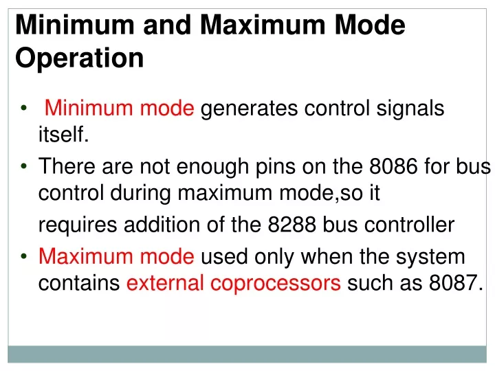
Minimum and Maximum Mode Operation • Minimum mode generatescontrol signals itself. • There are not enough pins on the 8086 for bus control during maximum mode,so it requires addition of the 8288 bus controller • Maximum mode used only when the system contains external coprocessors such as 8087.
The 8288 Bus Controller • Provides the signals eliminated from the 8086/8088 by the maximum mode operation. Figure 9–21The 8288 bus controller; (a) block diagram and (b) pin-out.
8288 Bus Controller Pin FunctionsS2, S1, and S0 • Status inputs are connected to the status output pins on 8086/8088. • three signals decoded to generate timing signals CLK • The clock input provides internal timing. • must be connected to the CLK output pin ofthe 8284A clock generator
8288 Bus Controller Pin FunctionsALE • The address latch enable output is used to demultiplex the address/data bus. DEN • The data bus enable pin controls the bidirectional data bus buffers in the system. DT/R • Data transmit/receive signal output to control direction of the bidirectional data bus buffers.
8288 Bus Controller Pin FunctionsAEN • The address enable input causes the 8288 to enable the memory control signals. CEN • The control enable input enables the command output pins on the 8288. IOB • The I/O bus mode input selects either I/O bus mode or system bus mode operation.
8288 Bus Controller Pin FunctionsAIOWC • Advanced I/O write is a command output to an advanced I/O write control signal. IORC • The I/O read command output providesI/O with its read control signal. IOWC • The I/O write command output provides I/O with its main write signal.
8288 Pin FunctionsAMWT • Advanced memory write control pin provides memory with an early/advanced write signal. MWTC • The memory writecontrol pin provides memory with its normal write control signal. MRDC • The memory readcontrol pin provides memory with a read control signal.
8288 Bus Controller Pin FunctionsINTA • Theinterrupt acknowledge output acknowledges an interrupt request input applied to the INTR pin. MCE/PDEN • The master cascade/peripheral data output selects cascade operation for an interrupt controller if IOB is grounded, and enables the I/O bus transceivers if IOB is tied high.
SUMMARY • Both 8086 and 8088 require a single +5.0 V power supply with a tolerance of ±10%. • The 8086/8088 microprocessors are TTL-compatible if the noise immunity is derated to 350 mV from the customary 400 mV. • The 8086/8088 microprocessors can drive one 74XX, five 74LSXX, one 74SXX, ten 74ALSXX, and ten 74HCXX unit loads.
SUMMARY (cont.) • The 8284A clock generator provides the system clock (CLK), READY and RESET synchronization. • The standard 5 MHz 8086/8088 operating frequency is obtained by attaching a 15 MHz crystal to the 8284A clock generator. • The PCLK output contains a TTL-compatible signal at one half the CLK frequency.
SUMMARY (cont.) • Whenever the 8086/8088 microprocessors are reset, they begin executing software at memory location FFFF0H (FFFF:0000) with the interrupt request pin disabled. • Because the 8086/8088 buses are multiplexed and most memory and I/O de-vices aren't, the system must be demultiplexed before interfacing with memory or I/O.
SUMMARY (cont.) • Demultiplexing is accomplished by an 8-bit latch whose clock pulse is obtained from the ALE signal. • In a large system, the buses must be buffered because the 8086/8088 microprocessors are capable of driving only 10 unit loads, and large systems often have many more.
SUMMARY (cont.) • Bus timing is very important to the remaining chapters in the text. A bus cycle that consists of four clocking periods acts as the basic system timing. • Each bus cycle is able to read or write data between the microprocessor and the memory or I/O system.
SUMMARY (cont.) • The 8086/8088 microprocessors allow the memory and I/O 460 ns to access data when they are operated with a 5 MHz clock. • Wait states (Tw) stretch the bus cycle by one or more clocking periods to allow the memory and I/O additional access time. • Wait states are inserted by control-ling the READY input to the 8086/8088. READY is sampled at the end of T2 and during Tw.
SUMMARY (cont.) • Minimum mode operation is similar to that of the Intel 8085A microprocessor, whereas maximum mode operation is new and specifically designed for the operation of the 8087 arithmetic coprocessor. • The 8288 bus controller must be used in the maximum mode to provide the control bus signals to the memory and I/O.
SUMMARY • This is because the maximum mode operation of the 8086/8088 removes some of the system's control signal lines in favor of control signals for the coprocessors. • The 8288 bus controller reconstructs these removed control signals.