Download
1 / 20
210 likes | 258 Views
This module presents a CryoPAF system using Xilinx RFSoC platform for direct digitization at focus. It integrates high-speed digital and RF subsystems with powerful processing capabilities. The compact "Jimble" design offers low EMI and reusability in various applications, with optical and electrical interfaces. The hardware overview includes power sequencing, signal conditioning, and features such as sample clock synthesis and packet processing. The prototype achieves high shielding effectiveness and thermal impedance, housed in a compact enclosure for efficient signal processing and data transmission. Verification includes EMI testing and design optimization for multi-channel signal processing. The system utilizes minimal power and resources, ensuring high efficiency and ease of integration in astronomical applications.

E N D
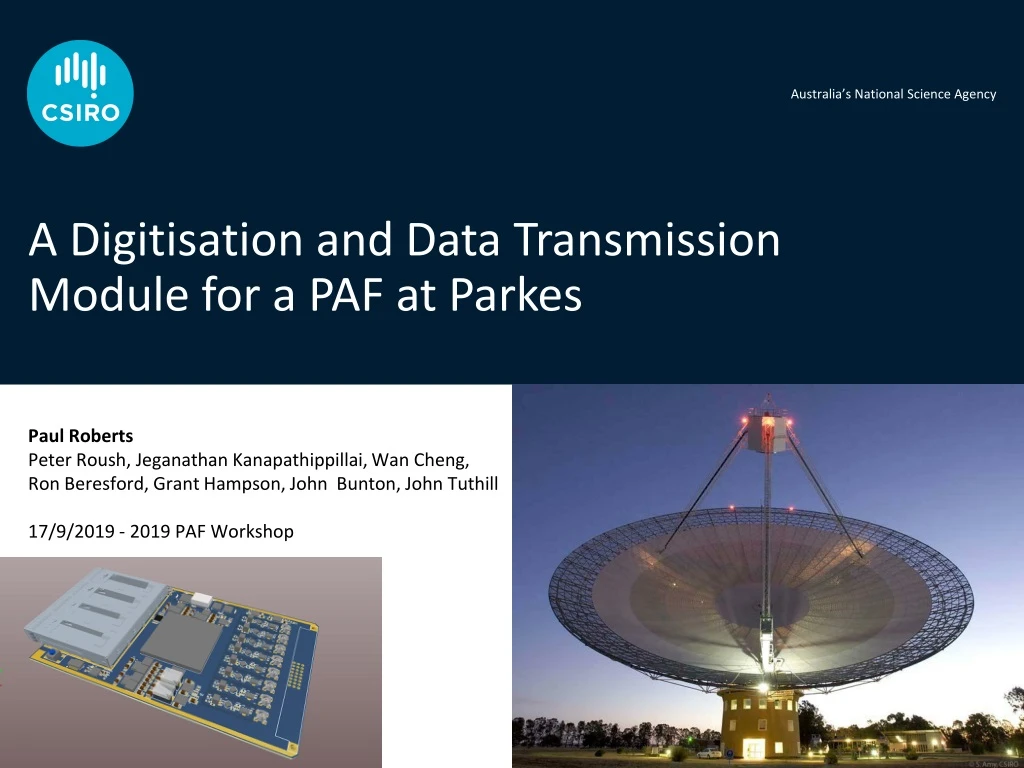
A Digitisation and Data Transmission Module for a PAF at Parkes Paul Roberts Peter Roush, Jeganathan Kanapathippillai, Wan Cheng, Ron Beresford, Grant Hampson, John Bunton, John Tuthill 17/9/2019 - 2019 PAF Workshop
System Architecture Warm RF Electronics Digitiser PAF Cryostat ~200m 1 GbE 100Gb Packet Data 128MHz & Time Frame Beamformer Timing Reference and Distribution Control & Monitor 10MHz 1PPS GPU Cluster Baseband RF input Direct digitisation at focus Packetised digital data transmitted Need a high integration solution=> RF to Packet Data
Xilinx RFSoC Platform – An FPGA plus more. • Four major parts to RFSOC: • Digital-RF subsystem (ADC/DAC) • Programmable logic (FPGA core fabric) • Processor System (ARM Cortex) • SerDes interfaces (high speed serial IO) • Powerful combination of four technologies in one. • High integration, performance and cost savings • Gen-1 • 16 x 2GSPS ADCs • 8 x 4GSPS ADCs
“Jimble” Board Design Philosophy 3.5cm • Simple – remote ADC/Packetiser/Transmitter applications • Small but powerful like namesake • C.f. “Bluering” for more capability • Low EMI – attention to EMI and no local CPU/DRAM etc • Reusable in other applications – 3U 100x160mm reconfigurable form factor • Data/Timing/Reference/Control interfaces – Fully optical (optional electrical) • Only electrical inputs are RF and power • Command and control 1/10 GbE
12V “Jimble” Module Hardware Overview Power Sequencing Power QSFP Signal Conditioning RF Input Xilinx RFSoC XCZU27DR QSFP 100 Gb Aurora/Enet x8 total QSFP 1GbE Signal Conditioning RF Input Buffer Amp BAT QSFP Sample Clock Synths Reference, Timing & Control VCXO Clean-up Ref 128MHz
“Jimble” Module Signal Processing Overview RF1 ADC 12bit 4.096 GS/s Packetise and Time stamp Over-sampled PDFB ~1MHz Channels 100 Gb PHY RF2 ADC 12bit 4.096 GS/s Packetise and Time stamp Over-sampled PDFB ~1MHz Channels Packet Mux and Scheduling Engine 100 Gb PHY 100 Gb PHY RF8 ADC 12bit 4.096 GS/s Packetise and Time stamp Over-sampled PDFB ~1MHz Channels
Initial Prototype results: 120 dB shielding effectiveness measured Thermal impedance ~0.35 degC/W Housed in a combined RF/Digital isolated enclosure Form factor MTP12 Ribbon – WDM & single fibres
< 100 fs RMS jitter required for 60 dB ADC SNR Design verification – Sample clock and Timing ~200m fibre <30Hz BW 128MHz REF Sample Clock Synth 4.096GHz Jitter Cleaner Loop RFSoC SFP SFP ADC CLK E/O O/E 128MHz VCXO Manchester Encoded Time Frame SFP SFP Jimble Board Optical Reference Signal Distribution over (Q)SFP 70 fs rms (300Hz-100MHz)
Design verification – signal processing Packet Engine 100GbE PHY GPU Coarse DFB 122MHz Channels Selector ADC 3.93GS/s RF IN 100GbE Monitor 4096 Ch FFB + Spectrometer ZU28 RFSoC (ZCU111) On-chip 4k Spectrum 100GbE ZCU111 GPU spectrum of a 122MHz sub-band RF IN (50-4000MHz)
Full x8 input and x8 ADC/PDFB Design at full clock rate implemented on ZCU111 Uses ~ 25% of DSP48/Logic/BRAM resources – highly efficient reuse Plenty of available headroom for control and data transmission Power = ~40 W total - measured from supply current monitors on ZCU111 Design verification – multi-channel signal processing firmware
Design verification – EMI properties of board, Power supplies, enclosures Measured EMI of intended DC/DC converters EMI emissions of ZCU111 Measured spurious contamination on ZCU111 board with spectrometer Shielding effectiveness of various enclosure concepts
Design verification – POL DC-DC Converters Measured EMC of intended DC/DC converters - Evaluated multiple DC-DC converters - Settled on LT “Silent Switcher” family Photo: Ron Beresfod Silent Switcher
Design verification – ZCU111 RFSOC board emissions • Measured while running representative design. • DC-DC Converter noise • 122 MHz Reference comb • Highlights areas that need to be mindful of in board design
Design verification EMI – ZCU111 RFSOC board High Sensitivity Integrating Spectrometer • Noise input at nominal astronomy power level • Integrated spectra 5s across 122MHz sub-bands • No evidence of spurii in any sub-bands • Differential topology and careful screening. • Confidence a spurii free design can be • achieved.
Board Geometry and Layout Quad QSFP Clock RFSoC DIN41612 DC-DC Analogue Completion of first prototype expected Nov/Dec 2019
Where does the data go => 1GHz Beamformer Repeat 3 times - one for each RFSOC QSFP Gemini FPGA LRU 4 Tera-multiply-accumulates (TMAC), 1.3 Tera-bits-per-second comms, and 24GB DDR4 memory
Summary A CryoPAFRFSoC based digitiser and data transmitter design presented Reusable in various applications Design at an advanced stage of completion All critical subsections independently breaded-boarded and tested First hardware prototype end of 2019
Thank youQuestions Astronomy and Space Science Paul Roberts+61 2 9372 4365 Paul.Roberts@csiro.au