Download
1 / 72
720 likes | 886 Views
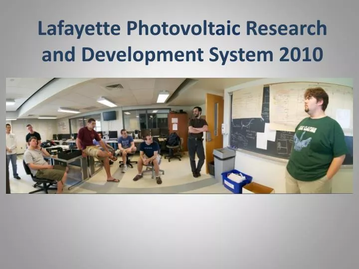
Lafayette Photovolt aic Research and Development System 2010. Presentation Outline. System Introduction Project Team System Block Diagram 2009 vs. 2010 Comparison 2010 System Focus Switch Controller (SC) Filter Inverter Box (FIB) Supervisory Control and Data Acquisition (SCADA)

E N D
Presentation Outline • System Introduction • Project Team • System Block Diagram • 2009 vs. 2010 Comparison • 2010 System Focus • Switch Controller (SC) • Filter Inverter Box (FIB) • Supervisory Control and Data Acquisition (SCADA) • Demo App and Tower Design • Safety Loop and Hardware • Project Status
What is the Lafayette Photovoltaic Research and Development System? • 2kW solar energy system that converts high voltage DC to 120V AC RMS signal of 60Hz • A test space for students to learn about energy issues and power engineering. • Subject to a Statement of • Work • Commercial Grid Tie Inverter • Requirements based team • oriented capstone project PV Array
Main Requirements • Automatic charge and discharge the LiFePO4 batteries • Delivery of 120V RMS, 60Hz ± 0.05% AC • Monitor, store and display real time temperature, voltage, and current data from all subsystems • Safety precautions to safely shut down the system if a fault is detected
Presentation Outline • System Introduction • Project Team • System Block Diagram • 2009 vs. 2010 Comparison • 2010 System Focus • Switch Controller (SC) • Filter Inverter Box (FIB) • Supervisory Control and Data Acquisition (SCADA) • Demo App and Tower Design • Safety Loop and Hardware • Project Status
Project Team • Began in 2009 with a 22 student and 2 professor team • 2010 team consists of 14 students along with the 2 original professors. • Over 40 people have contributed to this project
Systems Engineering Exposure • Much of today’s engineering is system engineering • System architecture issues • Interface design and documentation • Configuration management • Scheduling • Opportunity to manage complexity
Other Engineering Exposure • Exposure to mechanical issues • Most ECEs have little exposure to mechanical issues • Board layout • Subsystem Box layout • Assembly drawings • Exposure to safety issues • Safety lecture • Safety plan • Students limited to 30V • Lock out tag out • Must design with safety in mind! • High voltage isolation • HV/LV separation
Presentation Outline • System Introduction • Project Team • System Block Diagram • 2009 vs. 2010 Comparison • 2010 System Focus • Switch Controller (SC) • Filter Inverter Box (FIB) • Supervisory Control and Data Acquisition (SCADA) • Demo App and Tower Design • Safety Loop and Hardware • Project Status
System Block Diagram - PV • PV Array converts solar energy to electrical energy
System Block Diagram - RPI • The RPI Accepts high voltage DC from the PV array and delivers it to the rest of the system • Main safety hub
System Block Diagram - ESS • Battery Bank consisting of 64 3.2V Lithium Iron Phosphate Batteries • Creates 12V for other systems
System Block Diagram - FIB • Receives high voltage DC and converts it into a 120V RMS sinusoidal AC signal of 60 Hz
System Block Diagram - SC • Regulates the high voltage path between the PV, batteries (ESS), and the filter/inverter (FIB)
System Block Diagram - SCADA • Higher-level operation • Data collection of the other subsystems.
Presentation Outline • System Introduction • Project Team • System Block Diagram • 2009 vs. 2010 Comparison • 2010 System Focus • Switch Controller (SC) • Filter Inverter Box (FIB) • Supervisory Control and Data Acquisition (SCADA) • Demo App and Tower Design • Safety Loop and Hardware • Project Status
2009 to 2010 Major Changes • Power management algorithm (SC) • Working inverter/filter • Integrated SCADA • Demonstration application
Presentation Outline • System Introduction • Project Team • System Block Diagram • 2009 vs. 2010 Comparison • 2010 System Focus • Switch Controller (SC) • Filter Inverter Box (FIB) • Supervisory Control and Data Acquisition (SCADA) • Demo App and Tower Design • Safety Loop and Hardware • Project Status
System Testing • Subsystem QA • Low Voltage Testing • Basic System Functionality • Battery Management • High Voltage Testing • Reliability and Maintainability
Switch Controller (SC) • Regulates the high voltage path between the PV, batteries (ESS), and the filter/inverter (FIB) Student Designed Data Acquisition PCB Board Student Designed Box Layout and Wiring Scheme
BATT MGMT APP STATE TRANSITION DIAGRAM SoC Thresholds: 100% = 235V 65% = 205V 55% = 195V 20% = 165V
Low Voltage Testing Connect the system for DC Load Integration PV DC Source Disconnect FIB DC Load
Low Voltage Testing-Basic Functionality • Force LPRDSthrough all possiblestate transitions • Attempt illegal statetransitions
Low Voltage Testing-Battery Management • Force the SCthrough allpossible statetransitions • Two transitionsshould notoccur
Reliability and Maintainability Test Run the DC Load Integrated system for 24 hours • No unexpected faults or failures occur • No components overheat
Presentation Outline • System Introduction • Project Team • System Block Diagram • 2009 vs. 2010 Comparison • 2010 System Focus • Switch Controller (SC) • Filter Inverter Box (FIB) • Supervisory Control and Data Acquisition (SCADA) • Demo App and Tower Design • Safety Loop and Hardware • Project Status
Filter Inverter Box (FIB) Student Designed H Bridge PCB Board Student Designed Low Pass Filter Student Programmed Microcontroller • Receives high voltage DC and converts it into a 120V RMS AC signal of 60 Hz • Consists of: • H-Bridge • Low Pass Filter • Microcontroller FIB PICTURE Student Designed Box Layout and Wiring Scheme
AC Inverter • 4 high power insulated • gate bipolar transistors • (IGBT’s) in H-bridge • Allows voltage to be alternated in opposite directions to create sine wave • Microcontroller controls IGBT inputs by Pulse Width Modulation
Filter/Transformer • Filter • Removes switching frequency • THD of less than 3% required • Transformer • Reference output of FIB to building ground • Isolates the connection to the load
FIB Testing Requirements • Frequency = 60Hz ± .05% • Amplitude = 120Vrms ± 5% • Total Harmonic Distortion (THD) < 3% • Conducted emissions requirement of average Amplitude at 150KHz < -54dB and peak at 150KHz of < -41dB
Frequency Testing • Test setup • Oscilloscope with inputs from: • Signal generator • Differential output of filter • Hold one waveform on scope and time a full cycle of the other waveform across the first waveform • The inverse of this time is the frequency difference
Frequency Results • Time • 204s • Frequency difference • 1/204s • .0049Hz • Spec: 60Hz±.05% • Measured: +0.008% • Result………..PASS
Amplitude Testing • Set power supply to nominal battery voltage (205Vdc) • Plug in wall transformer to output of system • Measure the RMS voltage on oscilloscope • Scale by factor of transformer • Specification: 120VACrms ± 5% • Result: 119VAC ….……………………………….. PASS
THD Testing • Capture waveform on digital oscilloscope • Import data into MATLAB • Write program to calculate THD • Run program • Specification: 3% THD
THD Results THD calculated to be .157%.......................................................................PASS
Conducted Emissions Testing • Capture data on a digital oscilloscope • Import data into MATLAB • Calculate the FFT from the output waveform • Examine results above 150KHz
Conducted Emissions Results Peak at -16.93dB…………………………………………………………………………………Inconclusive
Presentation Outline • System Introduction • Project Team • System Block Diagram • 2009 vs. 2010 Comparison • 2010 System Focus • Switch Controller (SC) • Filter Inverter Box (FIB) • Supervisory Control and Data Acquisition (SCADA) • Demo App and Tower Design • Safety Loop and Hardware • Project Status
Supervisory Control and Data Acquisition (SCADA) • Controls higher level operation and collects data from each subsystem • State Manager App • Battery Management App • Maintenance App • Demo App