Download
1 / 18
230 likes | 449 Views
Research Opportunities in Laser Surface Texturing/Crystallization of Thin-Film Solar Cells Y. Lawrence Yao Columbia University January 4 th , 2011. Outline. Overview of Photovoltaic (PV) Technology Optical Confinement Methods Laser Surface Texturing (LST) Applications

E N D
Research Opportunities in Laser Surface Texturing/Crystallization of Thin-Film Solar Cells Y. Lawrence Yao Columbia University January 4th, 2011 Research Opportunities in Energy Manufacturing 2011 CMMI Grantees Conference
Outline Research Opportunities in Energy Manufacturing 2011 CMMI Grantees Conference Overview of Photovoltaic (PV) Technology Optical Confinement Methods Laser Surface Texturing (LST) Applications Simultaneous texturing/crystallization of a-Si:H thin films Research Opportunities
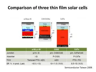
Comparison of PV Absorbers Thin Films Research Opportunities in Energy Manufacturing 2011 CMMI Grantees Conference
Performance Gaps in Efficiency Performance gaps between best device efficiencies in the lab and attainable efficiencies for several solar cell technologies (Kazmerski, 2005) Research Opportunities in Energy Manufacturing 2011 CMMI Grantees Conference At ~1.4eV highest attainable -III-V (GaAs) Si: 1.12eV a-Si:H – 1.7eV a-Si:H – largest potential gain in
Research Opportunities in Energy Manufacturing 2011 CMMI Grantees Conference
Overview of Solar Cells Research Opportunities in Energy Manufacturing 2011 CMMI Grantees Conference Thin films of more interest due to the large-area manufacturing feasibility a-Si:H has the lowest cost, however, it also suffers low efficiency and instability (the Staebler-Wronski Effect) GaAs has the highest efficiency, however, it costs 1000 times to make as other thin film absorbers III-V compound based multi-junction + concentrator can achieve the best efficiency (42.4%)
Optical Confinement Methods KOH (c-Si) (D. Heslinga, 2008) HF and HNO3 (polyc-Si) (D. Heslinga, 2008) Research Opportunities in Energy Manufacturing 2011 CMMI Grantees Conference • Anti-reflection coating (ARC) • Universally used • Chemical etching/texturing • Anisotropic alkaline and isotropic acid • Not applicable for amorphous and thin films • Mechanical texturing • Use mechanical dicing saws and blades - damage
Optical Confinement Methods Plasma (c-Si) (D. Heslinga, 2008) Acid 2 Acid 1 Research Opportunities in Energy Manufacturing 2011 CMMI Grantees Conference • Reactive ion etching • Low throughput • Laser surface texturing • Sharper surface features • Better absorption • More uniform absorption • Low throughput not easy for scaling up
LST Applications Research Opportunities in Energy Manufacturing 2011 CMMI Grantees Conference Tribology Biological Other applications in PV
Beyond Light Trapping (c-Si) Conduction band Energy Band gap Sub dopant band Valence band • SF6, (b) N2, (c) Cl2, (d) air, (e) vacuum • all used fs laser Carey, PhD Thesis, Harvard, 2004 Research Opportunities in Energy Manufacturing 2011 CMMI Grantees Conference • LST of c-Si in different atmosphere • Below-band-gap abs.
Beyond Light Trapping (c-Si) c-Si, SF6, Crouch et al ,2004 • fs laser: recessed surface, smaller pitch (2 to 3 times of , interference), ns laser: protruded surfaced, larger pitch (capillary wave generation) • Below-band-gap absorption: ns-laser allows higher doping concentration; annealing diffuses out dopants Research Opportunities in Energy Manufacturing 2011 CMMI Grantees Conference
a-Si:H Thin Films 800nm, 130fs, 0.4J/cm2 Film thickness 1.6 µm 248nm, 30ns, 0.4J/cm2 Film thickness 1.6 µm • Feasible for thin films • Below-band-gap absorption enhancement without dopant • nc-Si layer (1,100 nm) • Increased defects H. Wang, et al, 2009 Research Opportunities in Energy Manufacturing 2011 CMMI Grantees Conference
nc-Si layer in a-Si:H film Cross-section TEM fs laser sample Cross-section TEM ns laser sample • Texturing and surface crystallization in one step (XRD, TEM, EBSD) • ns laser induces more crystallinity • Potential for stability improvement • Crystalline structure to be further studied • Cavities in ns laser to be studied ns laser sample H. Wang, et al, 2009 Research Opportunities in Energy Manufacturing 2011 CMMI Grantees Conference
Research Needs Research Opportunities in Energy Manufacturing 2011 CMMI Grantees Conference • The one-step surface texturing/crystallization of thin film • Understand laser type and process conditions on resultant crystalline structures • Understand how the partial crystallization affecting stability of a-Si:H cells • Simultaneous doping (e.g., sulfur) –how does doping affect a-Si:H (minority carrier mobility and lifetime)
Research Needs Research Opportunities in Energy Manufacturing 2011 CMMI Grantees Conference • How to apply LST on III-V (e.g., GaAs) and multijunction cells • MOCVD for crystalline GaAs thin films is very expensive • Low-cost MBD for amorphous GaAs is much cheap –LST to surface texturing and crystallization • To address the high sensitivity to impurities introduced during the process
Research Needs Research Opportunities in Energy Manufacturing 2011 CMMI Grantees Conference • How to apply LST on III-V (e.g., GaAs) and multi-junction cells (cont.) • LST can potentially be used for texturing+crystallization+junction doping as a one-step process for each junction • Issues associated with complete crystallization throughout film thickness instead of partial crystallization • Effects of the tunnel junctions
Research Needs (R. Delmdahl, et al,2010) Research Opportunities in Energy Manufacturing 2011 CMMI Grantees Conference • Large-area, high-throughput LST • Effects of spatial and temporal characteristics of laser irradiation • Spatial: Homogeneous intensity/mask projection
Research Needs Research Opportunities in Energy Manufacturing 2011 CMMI Grantees Conference • Temporal: • longer laser pulse-width for crystallization • Double-peak pulse for high-throughput crystallization • But to address issues associate with increased HAZ and hydrogen explosion