Download
1 / 11
120 likes | 317 Views
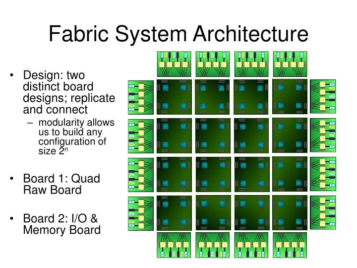
Fabric System Architecture. Design: two distinct board designs; replicate and connect modularity allows us to build any configuration of size 2 n Board 1: Quad Raw Board Board 2: I/O & Memory Board. The Saman Flip. How do we use the same board designs for every position in the fabric?

E N D
Fabric System Architecture • Design: two distinct board designs; replicate and connect • modularity allows us to build any configuration of size 2n • Board 1: Quad Raw Board • Board 2: I/O & Memory Board
The Saman Flip • How do we use the same board designs for every position in the fabric? • Quad board • symmetric in both dimensions • IO Board • symmetric about x-axis • compensate for board flip in firmware
Quad Board • 4 RAW chips per board • 16 152-pin MICTOR connectors total (4 per side) • Power distributed over separate cables from other signals • Connectors are stacked to save space
11” 11” Quad Board Layout Anant, I created the graphic in the previous slide to overlay exactly on this one. Their placement on the slide is also the same. I recommend fading from the previous slide to this one, so the audience can make the conceptual leap from the block diagram to the real layout.
I/O & Memory Board • 4 FPGAs • 2 64-bit PCI slots • 2 Expansion Ports (same as on Raw Handheld board) • 4 SDRAM banks • symmetric design (thanks Saman!) 11”
Clock Distribution from external input • Synchronized clocks for all Raw chips in fabric • Delay-Locked Loop uses feedback to tune delay line for clock synchronization • Dip switches keep clock dist. general no custom firmware
Power Distribution • 48V distributed to all boards, then down-converted • DC-DC converters on each board • 1.8V Raw core • 1.5V Raw I/O • 3V other logic • 1.5V is also further down converted to 0.75V supply for HSTL termination • System-wide power supply can be up to 3kW
Power Distribution power supply • distributed separately from signals • external power supply feeds top and bottom rows of I/O Boards
Clock Distribution clock generator • signal generated and distributed from a center board over MICTOR connectors • uses PLLs to deskew the clock at each connection • every quad board sends and receives a copy of the clock to its neighbors and we can select which of the input clocks to use using dip switches
Reset Distribution • signal generated by one of the I/O boards and distributed over MICTOR connectors reset originates here