Download
1 / 17
170 likes | 186 Views
This research presentation discusses the radiation hardness of 3D silicon and planar devices, exploring factors like charge collection, radiation damage, and bulk defects. The study compares the efficiency and reliability of 3D silicon structures at high fluences, highlighting the importance of signal formation, charge diffusion, and noise reduction. Implications for future detector designs and radiation tests are also considered.

E N D
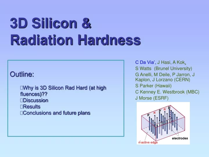
3D Silicon & Radiation Hardness • Outline: • Why is 3D Silicon Rad Hard (at high fluences)?? • Discussion • Results • Conclusions and future plans C Da Via’, J Hasi, A Kok, S Watts (Brunel University) G Anelli, M Deile, P Jarron, J Kaplon, J Lorzano (CERN) S Parker (Hawaii) C Kenney E. Westbrook (MBC) J Morse (ESRF)
OBVIOUS ANSWER is ‘yes because 3D has’: • Short collection distance (50 mm) • High average e-field with moderate Vbias • Parallel charge collection • Always use full substrate thickness (MIP ~80 e-/mm) • Drawback: higher Capacitance (measured 200 fF/121mm/electrode) Could thin [O] rich planar Silicon devices be competitive? IWORID 2004 C. Da Via Brunel University
3D VERSUS PLANAR microcracks, chips induce surface leakage current particle Active edge PLANAR 3D ~ 500mm p+ p+ n+ n+ 50 mm i - - 300 mm - - - - - - - - + + + + + + + + + + n+ Collecting electrode Collecting electrode p n MEDICI simulation of a 3D structure n n Drift lines parallel to the surface IWORID 2004 C. Da Via Brunel University From H Spieler/LBL, data from Radeka/ BNL
total n p other charged hadrons RADIATION DAMAGE IN HIGH ENERGY PHYSICS EXPERIMENTS: Multiple particle environment >85% charged Hadrons for pixels 1MeV neutron eq ATLAS Feq R=4cm 1.6x10¹⁶ NIEL compilation due to G. Lindstrom, NIEL IS VIOLATED between n and p when high [O] in Si ~5x10¹⁵ ~5x10¹⁴ IWORID 2004 C. Da Via Brunel University
RADIATION INDUCED BULK DAMAGE in Si Primary Knock on Atom Displacement threshold in Si: Frenkel pair E~25eV Defect cluster E~5keV Vacancy Interstitial Van Lint 1980 IWORID 2004 C. Da Via Brunel University
Studies mainly from RD48/ROSE Collaboration AT 1x10¹⁵ n/cm2 : STANDARD 300mm n-type SILICON at 1015 n/cm2 10 years of operation at L=1034 cm-2s-1 at R=4 cm EFFECTIVE DRIFT LENGTH Due to charge trapping~150mm e- ~50mm h SPACE CHARGE-ve Neff (1013/cm3) ~ VFD (5000V)~F TYPE INVERSIONdepletion from n-contact (e-field) REVERSE ANNEALINGINCREASE OF -ve Neff temp. dep LEACKAGE CURRENT prop to F (I/V ~5x10-17F) • Signal formation • Charge sharing • Speed • Double junction • Charge diffusion • Noise • Thermal runaway Time [y] • Maintenance IWORID 2004 C. Da Via Brunel University
V+O = VO EFFICIENT TRAPS! V2+0 = V2O CONTRIBUTES TO NEFF NEUTRON PROTON PUZZLE PROTONS POINT DEFECTS Signal can degrade because of: reduced depleted volume trapping IWORID 2004 C. Da Via Brunel University
EXAMPLE OF NIEL VIOLATION Effective trapping time tt for e and h measured by Kramberger differs between neutronand proton irradiation Leff = tt x vdrift • Collect electrons • Beware protons! • Work at vdrift saturated Trapping times from Kramberger et al. NIMA 481 (2002) 100 Simulations CDV and S.Watts NIM A 501(2003) 138 (Vertex 2001) IWORID 2004 C. Da Via Brunel University
25ns electronics 3x10¹⁴ n/cm2 T=-170C Casse’ et al. NIMA 487 (2002) 465-470 CONSIDERATION ON CCE and SIGNAL 2 REGIMES: 1- LOW FLUENCE- DEPLETION VOLUME DOMINATES Neutrons= bad Protons =good Oxygen helps 2- HIGH FLUENCE –TRAPPING DOMINATES Neutrons = bad Protons = worse! Oxygen does not help 500 n-in-p 400 300 Oxy p-in-n 200 Standard p-in-n 100 0 0 100 200 300 400 500 600 IWORID 2004 C. Da Via Brunel University
THE SIGNAL IS DIRECTLY PROPORTIONAL TO Leff Positive! The signal flattens at high f Should then planar detectors be thinner? data strip pad IWORID 2004 C. Da Via Brunel University
50 mm e- ONLY IF PITCH PROP. SMALLER 1 pad 50 mm If same pitch Thin detector = PAD! Scale!! 0.07 Better to work under-depleted With a thicker detector to make use of the steepness of the weighting potential (which only depends on the electrode width/thickness ratio) Distance (cm) IWORID 2004 C. Da Via Brunel University
n+ p+ MIP 121 mm depletion 3D - RADIATION HARD TESTS Room Temperature NON oxygenated • VFD • CCE AFTER 1x10¹⁵p/cm2 (5x10¹⁴n/cm2) 105 V AFTER 2x10¹⁵ n/cm2 • IEEE Trans on Nucl Sci 48 (2001) 1629 • Nucl.Instrum.Meth.A509:86-91,2003 joined work Brunel, Cern, Hawaii to be published
1 0 -1 MIP -2 -3 -4 -5 -6 -7 -20 -10 0 10 20 ns SPEED (SLHC bx =12.5ns) MIP 3.5 ns at 300K before and after f 1.5 ns at 130K MIP MIP MIP After 1x10¹⁵p/cm2 (5x10¹⁴n/cm2) counts time [ns] *Fast Electronics CERN MIC : P. Jarron et al. NIM A 377 (1996) 435 IWORID 2004 C. Da Via Brunel University
3D wins compared with equal electrode spaced Si if pitch is not smaller despite larger 3D capacitance (thin substrate higher C in planar devices as well) • S/N better for 3D because one can use all the charge deposited in the substrate In Conclusion: A lot to do! At high fluences charged hadrons are lethal for trapping Oxygen does not help when trapping is dominating Signal depends on Leff and on 1/F Very inspiring article by Kramberger et al. NIM A 511 (2003)82
Forthcoming 3D tests: • ATLAS pixel compatible (radiation limit) • TOTEM 3 x 4 cm2 (pure 3D, planar with 3D edges) • Speed measurement with 0.13 µm CMOS • Radiation tests for active edge (planar/3D) IWORID 2004 C. Da Via Brunel University
Atlas Upgrade Pixel Cell Design 3 Collection and 3 Field electrodes per Cell Depletion Distance Under 75 mm Electrode Area 6 % of Cell (improved etching may reduce this)
3D – TOTEM • Full size active edge sensor 3 x 4 cm2 • Forthcoming tests at X5 and SPS