Download
1 / 15
170 likes | 311 Views
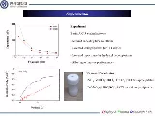
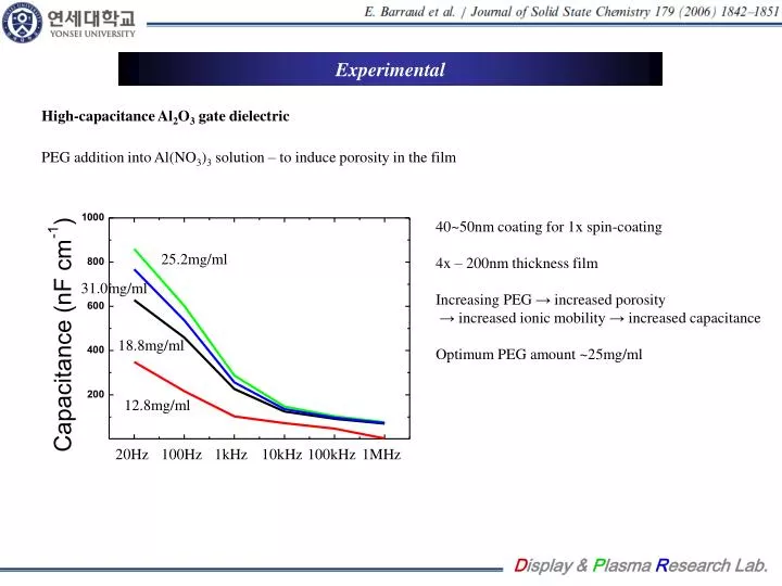
Experimental. High-capacitance Al 2 O 3 gate dielectric. PEG addition into Al(NO 3 ) 3 solution – to induce porosity in the film. 40~50nm coating for 1x spin-coating 4x – 200nm thickness film Increasing PEG → increased porosity → increased ionic mobility → increased capacitance

E N D
Experimental High-capacitance Al2O3 gate dielectric PEG addition into Al(NO3)3 solution – to induce porosity in the film 40~50nm coating for 1x spin-coating 4x – 200nm thickness film Increasing PEG → increased porosity → increased ionic mobility → increased capacitance Optimum PEG amount ~25mg/ml 25.2mg/ml 31.0mg/ml 18.8mg/ml 12.8mg/ml 20Hz 100Hz 1kHz 10kHz 100kHz 1MHz
Experimental High-capacitance Al2O3 gate dielectric 250˚C – decomposition of Al(NO3)3 but residual PEGs 1x coating PEG m.w. 6000 2x coating PEG m.w. 600 w/o PEG 20Hz 100Hz 1kHz 10kHz 100kHz 1MHz
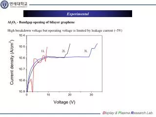
Experimental High-capacitance Al2O3 gate dielectric Thickness – 300 ˚C Significant enhanced capacitance (~3µF/cm2) Increased operating frequency up to 100Hz for thinnest film µm-thickness film was not required (capacitance saturates <50nm) → Sufficient proton 1x coating 2x coating 3x coating 20Hz 100Hz 1kHz 10kHz 100kHz 1MHz
Experimental High-capacitance Al2O3 gate dielectric Thickness – 350 ˚C Significant enhanced capacitance (~3µF/cm2) Increased operating frequency up to 100Hz for film thickness up to ~150nm 3x coating 1x coating 2x coating 20Hz 100Hz 1kHz 10kHz 100kHz 1MHz
Experimental Future works Solution-processed Al2O3 EDLdielectric Higher capacitance Solution processibility Practical thickness 1) To be comparable to ion-gel dielectric: > 10 µF/cm2 Increasing –OH, hydrolysis: - Water solvent - Low-temperature solution 2) To be comparable to ion-gel dielectric: > 100 µF/cm2 - Novel new idea - ex) BCP-templated: aligned pore structure To characterize: Porosity – ellipsometry Ion mobility – Impedence
Mechanics of Flexible Electronics Flexible IGZO TFT: Fail mode Crack in gate dielectric layer Delamination from polymer substrate 1 – Tensile strain 2 – Compressive strain Failure strain ~0.2%-0.4% for tensile strain ~0.8%-0.9% for compressive strain (similar to a-Si TFT)
Mechanics of Flexible Electronics Flexible IGZO TFT: Fail mode PolysiliconTFT on steel foil Tensile: Crack propagate from passivation oxide – start from edge, agrees well with finite element modeling Compressive: Delamination from steel foil substrate
Mechanics of Flexible Electronics Neutral axis engineering Pentacene TFT at neutral axis – Theoretically zero strain 0.5mm critical bending radius – from finite device thickness IDS decreases after 60,000 times, and finally decreases by 10% at 160,000 times
Mechanics of Flexible Electronics Flexible a-Si:H TFT with resilient insulator The transistor structures can be bent down to 0.5 mm radius (5% strain) in tension 1 mm radius (2.5% strain) in compression Shear deformation of hybrid layer Reduce strain of inorganic layer
Mechanics of Flexible Electronics Flexible pentacene TFT: with multilayer dielectric PVP : Mechanical flexibility HfO2: low leakage current Bending cycle: Increasing mobility Enhanced surface polarization of organic dielectric surface Doping effects caused by the accelerated chemical interactions of absorbed H2O and O2 molecules with the pentacene layers cracked by repetitive deformation Increasing PVP thickness → Less cracking at HfO2 layer 400nm GI was stable → Endure 105 bending cycles
Mechanics of Flexible Electronics Artificial Nacre: Layer-by-layer materials Abalone shell: Inorganic tiles slide instead of strain and the protein stretches to absorb the energy
Mechanics of Flexible Electronics Saponite- carboxymethylcellulose Na salt film High flexibility Thermal stability Flexible Transparent Clay Films Structure of clay After 350 ˚C, 1 hr
Mechanics of Flexible Electronics Experimental procedure Using soft material as a gate dielectric Clay-based method Synthesis: Saponite powder → Disperse to water → Add organic binder → Casting Limitations 1) Cannot enhance stretch-ability 2) Mechanical property is affected by humidity S/D depo. S GI G S GI G Transfer S S Flexible clay substrate GI GI G G PET PET
New paper 2DEG formation at LAO/STO interface VO formation to prevent polar catastrophe → 2D electron gas formation
New paper 2DEG formation at LAO/a-Al2O3 interface VO formation by oxidation of TMA on STO surface → 2D electron gas formation Possible application: HEMT Limitation: 100V at T= 4.2 K Research field: Superconducting oxide between insulator Magnetic effect between nonmagnetic oxide Interfacial metal-insulator transition Surface charge writing – memory device Enhancing high-k dielectric Interfacial Seeback effect