Download
1 / 13
130 likes | 225 Views
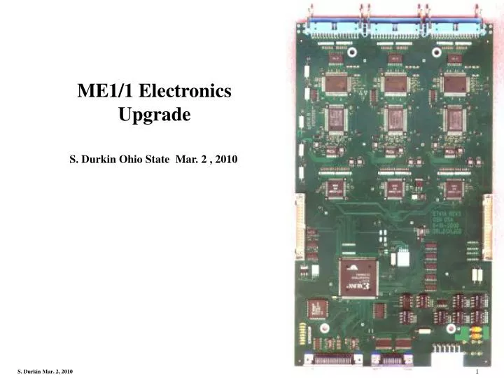
ME1/1 Electronics Upgrade S. Durkin Ohio State Mar. 2 , 2010. Digital CFEB – Designed for the SLHC. Deal with possible ME1/1 Rate Issues Replace Conventional ADC and SCA storage with Flash ADC and Digital Storage New System Deadtimeless , Removes rate worries

E N D
ME1/1 Electronics Upgrade S. Durkin Ohio State Mar. 2 , 2010 1
Digital CFEB – Designed for the SLHC • Deal with possible ME1/1 Rate Issues • Replace Conventional ADC and SCA storage with • Flash ADC and Digital Storage • New System Deadtimeless, Removes rate worries • Similar cost to old system • Fairly Radical Idea – Couldn’t build 5 Years Ago 2
ME1/1 Linked to ME4/2 Upgrade? • New ME4/2 chambers need boards. • Propose 514 new cards ME1/1 • Old cards to populate ME4/2 Upgrade • ME1/1 • Handles highest particle flux • Most important for momentum • resolution. • Removes ganged strips in ME1/1a • DCFEBs were designed for SLHC • Luminosity at SLHC unfortunately • years away. • A 1:1 swap with little immediate • improvement and risks involved • Don’t know rates yet • First do no harm… 3
Digital CFEB part a Large Electronic System ME1/1 Electronics Upgrade 514 DCFEBs OSU 0.5 FTE 72 DMBs 72 TMB (d.c.)TAMU+ULCA 1.0FTE 72 LVDB (+more power) 72 LVMB 1028 Cables (default skewclear) LVDB 2010 R&D Funding Build Roughly 1/6 of Present CMS Cathode System in 18-24 Months • Definitely Aggressive, Possible? Not with present manpower • Engineers need >18 months to design and build preproduction board, • and mass produce production boards (radiation tests…) • Time has to be allocated to test boards as system 4
Digital CFEB R&D Board Designed to study linearity, noise, data transmission(there will be issues): - Coupling single ended Buckeye Amp to bipolar flash SCAs - Fiber output versus Skewclear output Noise on Analog-Digital boards can be problems - use old PC boards analog isolation 5 Have started schematic and PC board layout Could have board in R&D board 4 months if no interruptions… Perform linearity tests, noise tests, and then Radiation testing in a beam
How long did present CFEB take to produce? CFEB 2 R&D boards, 2 preproduction boards 1997-2000 Test beams, Radiation tests (SEU rates, Total Dosage) CFEB production & testing October 2001-July 2003 2 Engineers/physicists , 2 Technicians, 1 Student • this time we expect to only need 1 R&D board • DCFEB Amplifier PC board noise protection copied from CFEB PC • CFEB production & testing faster with 1/5 number of boards 6
Conclusion Schedule set by LHC shutdown not by physics, R&D, or manpower • With additional engineer could produce R&D prototype by mid-summer • Manpower needs to be found to design and build other boards and cables • Time and physicists need to be found for board radiation tests as well • as testing the resulting prototype boards as a system Risks: Nearly Impossible Schedule to Meet We are willing to attempt it (with additional manpower) Must assure ME1/1 new electronics as good as old electronics Cannot rush board and system tests 7
First Step – Choose ADC • ADC choice drives subsequent design considerations • Interface between pre-amp and ADC • Voltage/Power requirements • Could impact LVDB design • ADC choices:(8 ch, 12 bit, 20-65 MSPS, Serial LVDS output) • MAX1437 (Maxim) 1.8V supply, 1.4Vpp range • ADC12EU050 (National) 1.2V supply, 2.1Vpp range • AD9222 (Analog Devices) 1.8V supply, 2Vpp range • ADS5281 (Texas Instr.) 3.3V analog, 1.8V digital, 2Vpp range 9
Issues with ADCs • None are suitable drop-in replacements for SCA/ADC • ADC’s • All have differential inputs • Limits on common mode • Have internal input bias network • Pre-Amp • Single ended output • Limited range of baseline level • Designed to drive small capacitive load • Pre-Amp/ADC Interface • Mnfr. suggest transformer coupling • (not an option for us) • Amplifier to generate differential signal • (requires 96 amplifiers) • Direct couple single ended signal • (common mode consequences) • (level shifting/scaling) • AC couple single ended signal • (common mode consequences) • (no level shifting, but still have biasing to consider) 10
Evaluation Boards • Purchased Evaluation Boards for ADS5281 and AD9222 • Basic Setup: Logic Analyzer Input Circuitry ADC DeSer + - • Identify constraints/operation limits of ADC • Direct Coupling Concerns • Common Mode • Data Sheet: Vcm = 1.5±0.05V • How far from nominal? • Baseline Level • Range • Digital output range is 2V • But is linear range of common mode 2V? • AC Coupling Concerns • Same as direct coupling • No worries with pre-amp baseline level • But need to bias positive input 11
Constraints (ADS5281) • ADC Constraints: • Vcm -600mV < (IN+ + IN-)/2 < Vcm +300mV (1.8Vpp on IN+) • (IN- -1V) < IN+ < (IN-+1V)(ADC output range) • Pre-Amp Constraints: • Baseline Level • Currently 1.8V • Max ~2.0V • Min ~1.2V (maybe 1.0V) • Drive Capability • Small (few mA at best) • Scaling: • Scale down input • Add digital gain on output • Resistor divider 1.2k Vcm 12 1.2k
Digitize Amplifier Pulses Connect CFEB to Evaluation Board: 13 50ns samples