Download
1 / 24
240 likes | 262 Views
This lecture discusses the different FPGA devices, their range of capabilities, architecture, and applications. Topics include fully SRAM-based configuration, configurable logic blocks (CLBs), input/output blocks (IOBs), and digital clock management blocks (DCMs).

E N D
Lectures 21, 22 FPGA and Top-Down Design Flow Mar. 3 and 5, 2003
What is an FPGA ? Fully SRAM based configuration Block Memory. • Configurable Logic Blocks (CLB) • Used to form adders, accumulators, multipliers, etc. Input/Output Blocks (IOB)
What a Range of Devices: Which One? • The lowest cost devices for DSP applications ($5 to $10) • 96 to 864 CLBs with up to 48k-bits RAM • The father device from which all Virtex devices have been derived • Rarely used for new designs • 384 to 6144 CLBs with up to 128k-bits RAM Cont’d on next slide
What a Range of Devices: Which One? • 384 to 16224 CLBs with up to 832k-bits RAM • For those particularly memory intensive algorithms • 2400 to 4704 CLBs with up to 1120k-bits RAM • 128 to 23,296 CLBs* with up to 3024k-bits RAM • Latest family and most DSP-focused FPGA architecture ever to be released *scaled to enable comparison
Xilinx FPGA Device Architecture • Uniform structure of programmable blocks, which can be connected together using programmable interconnect Fully programmable. Replace all functionality in <50ms Memory Blocks Input/Output Blocks (IOB) Configurable Logic Blocks (CLB) Digital Clock Management Blocks (DCM) Programmable Interconnect
Spartan-II • Spartan-II geared to high volume production • Memory blocks are located down each side of the device • Each memory block is 4 CLBs high • Since the area of CLBs increases more than the length of the two edges, the CLB to block memory ratio increases with larger devices XC2S15 = 24 CLB per Block RAM XC2S150 = 72 CLB per Block RAM
Contents of the Course ASIC FPGA • Transistor and Layout • Gate and Schematic • Systems and VHDL/Verilog
Contents of the Course (cont’d) 2 ASIC labs 2 FPGA labs • Transistor/Layout • Gate and Schematic • Systems/VHDL (Cadence) (Xilinx Foundation) (Synopsys)
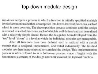
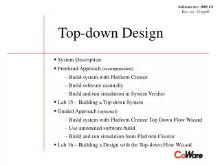
Xilinx Foundation Tutorial Lab 3: Top-down design Lab 4: Download to FPGA development board
Lecture 23 Driving Large Load Pass Logic Mar. 7, 2003
Driving large loads • Sometimes, large loads must be driven: • off-chip; • long wires on-chip. • Sizing up the driver transistors only pushes back the problem—driver now presents larger capacitance to earlier stage.
Optimal sizing • Use a chain of inverters, each stage has transistors a larger than previous stage. • Minimize total delay through driver chain: • ttot = n(Cbig/Cg)1/n tmin. • Optimal number of stages: • nopt = ln(Cbig/Cg). • Driver sizes are exponentially tapered with size ratio a.
Topics • Swtich logic.
Switch logic • Can implement Boolean formulas as networks of switches. • Can build switches from MOS transistors—transmission gates. • Transmission gates do not amplify but have smaller layouts.
Behavior of n-type switch n-type switch has source-drain voltage drop when conducting: • conducts logic 0 perfectly; • introduces threshold drop into logic 1. VDD VDD - Vt VDD
n-type switch driving static logic Switch underdrives static gate, but gate restores logic levels. VDD VDD - Vt VDD
n-type switch driving switch logic Voltage drop causes next stage to be turned on weakly. VDD VDD - Vt VDD
Behavior of complementary switch • Complementary switch products full-supply voltages for both logic 0 and logic 1: • n-type transistor conducts logic 0; • p-type transistor conducts logic 1.
Layout characteristics • Has two source/drain areas compared to one for inverter. • Doesn’t have gate capacitance.