Download
1 / 3
40 likes | 195 Views
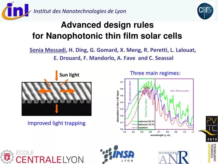
Advanced design rules for Nanophotonic thin film solar cells. Sonia Messadi , H. Ding, G. Gomard, X. Meng, R. Peretti, L. Lalouat, E. Drouard, F. Mandorlo, A. Fave and C. Seassal. Sun light. Institut des Nanotechnologies de Lyon. Three main regimes:.

E N D
Advanced design rules for Nanophotonic thin film solar cells Sonia Messadi,H. Ding, G. Gomard, X. Meng, R. Peretti, L. Lalouat, E. Drouard, F. Mandorlo, A. Fave and C. Seassal Sun light Institut des Nanotechnologies de Lyon Three main regimes: Improved light trapping
Sonia MESSADI Photovoltaic Technical Conference - Thin Film & Advanced Silicon Solutions 2013. Enhanced absorption by channeling at low wavelengths (blue) a-Si c-Si Electric field with and without conformal heterojunction • Effective index medium theories not suitable • Channeling in nanoholes: • larger absorption in underlying material • remaining absorption around holes : need for a good passivation 2
Modal Engineering at large wavelengths (red) Sonia MESSADI Photovoltaic Technical Conference - Thin Film & Advanced Silicon Solutions 2013. • Slow Bloch Mode critical coupling : coupling losses = absorption losses • Max peak absorption (50%) • Strong coupling of Slow Bloch Modes with incident plane wave: • Lower absorption peak value • Larger width • Larger integrated absorption Cf also “Absorption Enhancement in Disordered Photonic Crystals: A Photonics Point of View" - R. Peretti, Friday, 9:10 am • Process underway using bounded crystalline silicon thin films • In order to generate complex patterns, interferential lithography and dry etching can be used. 3