Download
1 / 12
160 likes | 503 Views
Characterization of CuInSe2 Thin Film Solar Cells. By. Chukwuemeka Shina Aofolaju 1 Advisors: Dr. Eric Egwu Kalu 1 Dr. Paul Salvador 2. 1. FAMU – FSU College of Engineering. 2. Carnegie Mellon University. Research Background.

E N D
Characterization of CuInSe2 Thin Film Solar Cells By Chukwuemeka Shina Aofolaju 1 Advisors: Dr. Eric Egwu Kalu 1 Dr. Paul Salvador 2 1. FAMU – FSU College of Engineering 2. Carnegie Mellon University
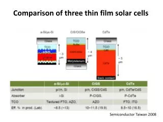
Research Background • Cost of Crystalline Silicon versus Fossil fuel electricity generation. • CIS thin films require less semiconductor material • They are potentially lighter and thinner than Silicon Solar Cells • CIS would be relatively inexpensive CIS – Copper Indium Diselenide
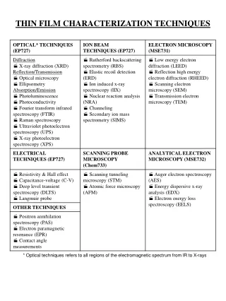
Hypothesis &Experimental Methods • Hypothesis: CIS deposition conditions influence the CIS film microstructure (atomic composition, film morphology) - affect of electrolyte flow rate • Experimental Methods • Atomic Force Microscopy • Views the surface profile of both CIS • X-ray Diffraction • Crystal structure and crystal orientation of the thin film particles • Scanning Electron Microscope (sample atomic composition)
Method of CIS Deposition • Substrate materials PET & Kapton. • Electroless Nickel is deposited on substrate • CIS Deposited on Electroless Nickel (non-recirculated and circulated bath) PET - poly(ethylene terephthalate)
Unannealed CIS AFM Scan Results Unannealed Samples Size: 50 um Roughness: 297 A Grayscale: 400 A Flow rate: 0.72 ml/s Size: 50 um Roughness: 334 A Grayscale: 540 A Flow rate: 0.85 ml/s 20 µm 50 µm 50 µm Annealed CIS Annealed Samples Size: 50 um Roughness: 194 A Grayscale: 140 A Flow rate: 0.72 ml/s Size: 50 um Roughness: 206 A Grayscale: 140 A Flow rate: 0.85 ml/s 50 µm 50 µm
X-ray Diffraction • Understand the molecular and material structure of the thin films • Monitor peaks and compare them to theoretical CIS scans • Note the differences or variation in peaks as flow-rate changes. • Scan annealed samples and see differences in peaks.
Result & Discussion • Peaks are present but are neither at the same angle of the theoretical CIS scans or intensity • CIS scans are similar to substrate scans (Mylar and Kapton) • Nickel scans are also similar to that of Mylar and Kapton • CIS not Crystalline.
SEM Results • Copper – 19.16 % • Selenium – 41.72 % • SEM Results show the presence of Copper and Selenium but no Indium. X-ray Diffraction analysis might not be the best way to characterize our samples OR Annealing factors should be changed to show crystalline structures.
Conclusion & Future Goals • Learned how to use the Atomic Force Microscope to view surface morphology of thin films • Studied the use of X-ray Diffractormeter and used it to characterize sample • Change the Annealing factors and find other methods to characterize samples. • Experiment through more flow rates.
Acknowledgements • CMU/FAMU PREM Program • Dr. Salvador and grad students • Dr. Eric Kalu • Miss Celina Dozier