Download
1 / 22
220 likes | 380 Views
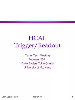
HCAL TPG and Readout. CMS HCAL Readout Status CERN Drew Baden University of Maryland June 2002 http://macdrew.physics.umd.edu/cms/ see also: http://tgrassi.home.cern.ch/~tgrassi/hcal/ And http://tgrassi.home.cern.ch/~tgrassi/hcal/CMSweek0301.pdf for TPG latency discussion. H T R.

E N D
HCAL TPG and Readout CMS HCAL Readout Status CERN Drew Baden University of Maryland June 2002 http://macdrew.physics.umd.edu/cms/ see also: http://tgrassi.home.cern.ch/~tgrassi/hcal/ And http://tgrassi.home.cern.ch/~tgrassi/hcal/CMSweek0301.pdf for TPG latency discussion
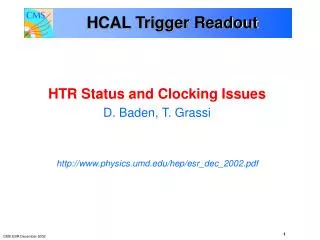
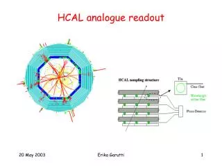
H T R H T R H T R DAQ RUI CCA CCA CCA HCAL FE/DAQ Overview “Trigger Primitives” (1.2 Gb/s) READ-OUT Crate (in UXA) DAQ DATA SLINK64 (1 Gb/s) Level 1 CAL REGIONAL TRIGGER CPU D C C 18 HTRs per Readout Crate 16 bits @ 80 MHz TTC 32 bits @ 40 MHz FRONT-END RBX Readout Box (On detector) HPD Shield Wall QIE GOL QIE QIE Fibers at 1.6 Gb/s 3 QIE-channels per fiber QIE GOL QIE QIE FE MODULE
Readout Crate Components • “BIT3” board • Commercial VME/PCI Interface to CPU • Slow monitoring • HTR (HCAL Trigger and Readout) board • FE-Fiber input • TPs output (SLBs) to CRT • DAQ/TP Data output to DCC • Spy output • TCC/Clock FanOut board • FanOut of TTC stream • FanOut of RX_CK & RX_BC0 for SLBs • DCC (Data Concentrator Card) board • Input from HTRs • Output to DAQ • Spy output Front End Electronics TTC fiber Gbit Ethernet @ 1.6 Gb/s F a n O u t B I T 3 H TR H T R H T R H T R D C C (s) ... D C C 20 m Copper Links 1 Gb/s DAQ Calorimeter Regional Trigger
Baseline 48 channel HTR • HTR consists of 2 identical 24-channel parts • Each “sub HTR”: • 8 TI TLK2501 transceivers • 3 HCAL channels/fiber • 2 x 8B/10B frames @ 80MHz = 1.6 Gbps • 4 Stratus dual LC optical receivers • Xilinx XCV1000E • Implements logic necessary for running • Level 1 (TPG) output via backplane to transition board • LVDS over backplane P2/P3 • P3 is a hard metric 5 row 47 pin connector used for DØ/CDF • 6 Synchronization Link Boards (SLB) for Tx to Level 1 • Developed at CERN for ECAL/HCAL VME
Dual LC Fiber Detector 8 TI TLK1501 deSerializers Xilinx XCV1000E FPGA Current Status HTR • HTR “Testbeam Prototype” now under test • Will be used in 2002 testbeam effort • Half functionality implemented: • 1 FPGA - Firmware in progress • 8 Deserializers Tested ok. • TLK2501 fussy (30-40ps pkpk jitter) • Experience: the closer Tx and REFCLK are to each other, the easier it is to link • DCC output – Tested ok. • External clock input – Tested ok. • VME – Tested ok. • 1.6 GHz link working • Tested at UMD and at FNAL with real FE • Clocking control issues and firmware shakedown get main consideration • System tests underway • Firmware written, all components under test • Full front-end to DCC path tested and working • VME path tested and working • Debugging, shakedown, etc. • ~10 more boards assembled by 21-JUN
Data Concentrator Card • PCI Motherboard design • All logic implemented on daughterboards • All I/O through daughterboards • Standard 33MHz PCI buses as interfaces • Motherboard design: DONE • Motherboards are in production • 5 prototypes are in hand for CMS • Receiver daughterboards: DONE • 10 2nd generation prototypes being built for testing • Logic motherboards: DONE • 2 prototypes in hand, waiting on final specs on DAQ link • Firmware for logic boards under test • No problems with this card • Technical, cost and schedule are all very good
DCC Prototyping Plans • Bandwidth tests and optimization • 240 MB/s vs. 264 MB/s max, maybe some gain still possible • Testing of DAQ event builder • DCC + 2 HTR working • This tests event building in DCC • Integration proceeding now, increasing in sophistication as we proceed. • Implement monitoring functions • Lots of “spy” buffers, access over VME, etc. • Tests of TTC input • Timing requirements not crucial for DCC since it is downstream of Level 1 accepts • Integration with HTR • Ongoing now • To be ready for testbeam effort
Optic Fiber Input VME64x connector Cat 5/RJ45 LVDS fanout TTCrx daughter card HCAL Fanout Prototype Board • Fanout card handles requirement for • TTC fanout • L1A/BC0 fanout for SLB synch • Clock cleanup for low jitter REFCLK • TTC Fanout • Each HCAL VME crate will have 1 TTCrx for all HTR cards • TTC signal converted to 120MHz LVDS, fanout to each HTR and over Cat5 w/RJ45 • L1A, BC0, CLK • Fanout using 40MHz LVDS • CLK is just for test/debugging • Clock Cleanup • Cleanup the incoming 80MHz TTC clock using VCXO PLL • Fanout to HTR • Status • Prototype board checked out ok • 3 production boards being checked out now. RMS jitter < 10ps after VCXO
Status HCAL/TriDAS Testbeam • Electrical: • Front-end HTR • Tests fiber link, especially clocking quality • Current scheme works, but we will learn more in battle • Plenty of redundancy built into the testbeam clocking system (see below) • HTR DCC • Tests LVDS channel link and data format on HTR • Tests LRBs on DCC and DCC PCI busses • So far no problems seen • HTR VME • Tests HTR VME firmware and internal data spy buffers • Tests successful, no problems forseen here (this is “easy”) • Clock fanout • Tests fanout board’s PLL/VCXO circuit and resulting jitter specs • <10ps RMS observed, corresponding BER for front-end data into HTR to be measured
Status HCAL/TriDAS Testbeam (cont) • Functionality • Firmware • HTR • Input FE data into SPY fifo out VME – tested ok, verification underway • Input FE data into DCC – tested ok, verification underway • TTCrx chip not yet tested – next few weeks • Ability to handle L1A correctly not yet tested – next few weeks • DCC • LRBs ok • 2 33MHz PCI busses ok • Event building (needs 2 HTR) ok so far, verification underway • Integration • FE HTR VME tested and working • Shakedown underway… • FE HTR DCC tested and working • Next tests will take data from DCC to CPU over S-LINK • FE HTR DCC SLINK CPU disk • With L1A, will use LED signal into QIE to test – next few weeks • Source calibration is via “streaming mode” – histograms will be made inside HTR FPGA
Clocking • Issues: • LHC beam collisions every 25 ns, large <n> necessitates pipeline • Data is transmitted from front-ends @ 40MHz over serial links • These links embed the clock in the data • Jitter on “frame” clock (1 frame = 20 bits) gets multiplied by “bit” clock • 80MHz frame clock, 1600MHz bit clock • Many clocks in HTR board • Best to describe in terms of “Tight” and “Relaxed” jitter requirement: • Tight jitter spec: 2 clocks needed • Reference clock for fiber deserializer chips needed to lock to incoming 1.6 Gbps data • 80MHz with 30-40ps pkpk max jitter to maintain lock • Provide transmitter clock for SLB output • 40MHz with 100ps pkpk max jitter at input to Vitesse transmitter • Loose jitter spec: 1 clock needed • TTC-derived system clock for HTR logic used only by FPGA to maintain pipeline • LHC clock comes into each VME crate and is fanned out using low jitter techniques to each HTR card
Quad Twisted Pair Cat 5 LVDS 40MHz RJ45 LVDS 120MHz Clock Implementation - HTR • Tight Jitter clock: • Use same clock for both 80MHz Serdes REFCLK and 40MHz SLB Tx clock • DFF used to divide 80MHz into 40MHz • Clock will be implemented in 2 ways: • Incoming from Clock Fanout Board • PECL fanout, convert to TTL at input to Serdes • Onboard crystal for debugging • Loose Jitter clock • Use TTC clock for 40MHz system clock • Clock will be implemented in 3 ways on HTR: • TTC clock from fanout board • External lemo connector • Backup input from fanout board • 2 RJ45 connectors with Cat 5 quad twisted pair connectors • 1st one has incoming low jitter 80MHz clock from fanout • 3.3V PECL on 1 pair, other 3 pair grounded • 2nd one has: • 120MHz LVDS TTC from fanout board on 1 pair • 40MHz LVDS L1A, Backup clock, and BC0 on other 3 pair L1A CLK BC0 TTC A/B Quad Twisted Pair Cat 5 RJ45 GROUND 80MHz CLK GROUND GROUND
HTR/Clock Implementation • In progress… Lemo test inputs….RST, L1A, CLK RJ45 connector with TTC, L1A, BC0, Clock_backup Fanout Buffer RJ45 connector with low jitter PECL 80MHz clock
Testbeam Clocking Scheme • UIC Clock Fanout Board • Fanout “clean” 80MHz PECL clock • Fanout TTC to all HTR via LVDS • 80MHz clean clock redundancy • HTR • 80MHz clean clock for Serdes REFCLK redundancy • 40MHz TTC sysclock, L1A and BC0 • Single clock source: 6U Princeton Clock Board • Source of clean 40MHz clock for TTCvx • Redundant 80MHz clock • TTCvx • Fiber output TTC 120MHz LVDS TTC 40MHz LVDS BC0/L1A/CLK REDUNDANCY Fiber 6U Clock Board Fanout Board TTC HTR Board SLB Transition Board LEMO 40MHz deserializers TTCrx LVDS TTCrx CLK “CLK” 1 to 8 Fanout BC0 L1A 80 MHz 80MHz 1 to 8 Fanout 80 MHz LVPECL Crystal 80 MHz PECL PECL 80MHz Clock Fanout 40 MHz REDUNDANCY Clean 80MHz Clock RJ45 Splitter REDUNDANCY
HTR Firmware Block Diagram • In progress…
HTR Firmware - VME • All firmware implemented using Verilog • Non Trivial firmware effort underway • 1 engineer, 1 EE graduate student, 1 professor • VME path to HTR uses Altera FPGA • BU is developing • Based on a “LocalBus” model • All devices are on LocalBus • 2 Xilinx FPGAs + 1 Altera • Flash eeprom (1 per Xilinx) for config over VME • TTC (trigger timing control) • 6 SLB daughterboards • VME and LocalBus implemented • VME kept simple - no DMA, interrupts, etc. MAIN FPGA 1 (Xilinx) Flash Eeprom 1 Altera 10k30 MAIN FPGA 2 (Xilinx) Flash Eeprom 2 VME FPGA (same 10k30) TTC SLB 1 SLB 2 SLB 3 VME SLB 4 SLB 5 SLB 6 LocalBus
HTR Firmware – HCAL functionality • Firmware for this consists of 2 paths: • Level 1 path • Raw QIE to 16-bit integer via LUT • Prepare and transmit trigger primitives • Associate energy with crossing • Extract muon “feature” bit • Apply compression • Level 2 path • Maintain pipeline with L1Q latency (3.2ms) • Handle L1Q result • Form energy “sums” to determine beam crossing • Send L1A data to DCC • Effort is well underway • 1 FTE engineer (Tullio Grassi) plus 1 EE graduate student plus 1 professor • Much already written, ~1000 lines Verilog • Much simulation to do • Focusing now on Level 2 path functions necessary for testbeam Schematic for each of 2 Xilinx FPGA
TPG Output to Level 1 • HTR cards will send data to Dasilva’s SLB boards • Quad Vitesse transmitter, 40MHz clean clock input (100ps jitter) • Mechanical considerations dictated design of 6-SLB transition board (SLB_HEX) • Baseline scheme: 6-SLB transition motherboard (SLB_HEX) • HTR will send 280 MHz LVDS across backplane • SLB_HEX will fanout 40MHz clean clock and have LVDS-to-TTL drivers • 6 SLB=48 TPG matches HTR “magic number” 3 HCAL channels/fiber input • Risks: lots of LVDS, but Dasilva is confident! • Alternate schemes under consideration • Move SLB’s to HTR • Mechanically challenging – heavy TPG cables • This is our main backup • Build 9U “super” SLB motherboard • Not sure if this helps…. • Build 6U crate of super SLB motherboards • Same thing….
1. Deserializers $500/card separate 2. Deserializers built-in Possible Changes to HTR • Change to newer Xilinx • Current chip XCV1000E • Vertex 2 – will • Advantages: • Half the cost, twice the memory • Almost pin compatible • Risks: • Issue of Block Ram cells • Vertex 2 PRO (0.13mm) • Advantages • Even lower cost • Built-in serializers, mechanical long term M&O advantage • Fewer I/O pins required, data arrives serially differential @ 1.6 GHz • Internal clock distribution. • Built in Motorola 300MHz PowerPC 405 • We will surely find a use for this! • 18-bit hardware multiplier per block ram • Risks: • This is a new part – we are working with the vendors to get engineering sample • Estimates for bulk orders to begin Nov 2002 • Pins – might not be enough for us • We will evaluate options this summer – Vertex 2 most likely
SLB SLB SLB SLB SLB SLB Possible Changes to HTR – TPG/TTC • TPG: • Baseline scheme: LVDS over backplane at 280 MHz • Advantages: • Level 1 cables are 20m impedance controlled for 1.2Gbps transmission • These are quite thick! • Backplane cards allow mechanical stability to be controlled • Note: Carlos Dasilva, already confirms baseline scheme works • Risks: • Noise and BER increase to unacceptable levels • Backup solution: move SLBs to back to HTR motherboard • Advantages: • No backplane transmission, easy to implement electrically • Saves 1 or 2 buckets in latency. • Risks: • Would necessitate complete rerouting of HTR board – schedule issue. • Evaluate in September Strain relief on front panel FPGA FPGA
Adding HO to RPC Trigger • Considerations: • Requirements • Trigger would only need 1 bit per HCAL tower • RPC trigger accepts 1.6 Gbps GOL output • Technical – how hard will it be to do this? • 48 channel HTR means 48 bits/HTR to RPC trigger • Each SLB twisted pair sends 24 bits @ 120MHz • Entire output could go via a single SLB • Can the SLB output be modified to drive fiber? • Can the RPC trigger receiver be modified to accept 1.2 GHz? • Under study….will try to come up with a decision this month • Mapping • HCAL mapping is very constrained (ask Jim Rohlf!) • Can we map our towers/fibers to the RPC? • Maybe easy for f • Maybe hard for h • Rohlf to study this….
Test Beam Jul-Sep Done FNAL source calib. Current HCAL/TriDAS Project Timeline 2001 2002 2003 2004 2005 June Sept Dec Mar Sep Apr Demonstrator HTR Firmware Development…. Pre-production Prototype Partial Install/Test/Burning ~10% (Includes “magnet test” period) 1.6 Gbps Link 9U Prototype Testbeam Firmware TPG Check 9U Proto HTR Production Alcove/Slice Integration April 03 to Nov 04 Full VertSlice Nov 04 to Apr 05 Beneficial Occupancy