Download
1 / 50
500 likes | 854 Views
Memories and the Memory Subsystem; The Memory Hierarchy; Caching; ROM. Memory: Some embedded systems require large amounts; others have small memory requirements Often must use a hierarchy of memory devices Memory allocation may be static or dynamic Main concerns [in embedded systems]:

E N D
Memories and the Memory Subsystem; The Memory Hierarchy; Caching; ROM
Memory: Some embedded systems require large amounts; others have small memory requirements Often must use a hierarchy of memory devices Memory allocation may be static or dynamic Main concerns [in embedded systems]: make sure allocation is safe minimize overhead
Memory types: RAM DRAM—asynchronous; needs refreshing SRAM—asynchronous; no refreshing Semistatic RAM SDRAM—synchronous DRAM ROM—read only memory PROM—one time EPROM—reprogram (uv light) EEPROM—electrical reprogramming FLASH—reprogram without removing from circuit Altera chips: http://www.altera.com/literature/hb/cyc/cyc_c51007.pdf memory blocks with parity bit (supports error checking) synchronous, can emulate asynchronous can be used as: single port—nonsimultaneous read/write simple dual-port—simultaneous read/write “true” dual-port (bidirectional)—2 read; 2 write; one read, one write at different frequencies shift register ROM FIFO flash memory: http://www.altera.com/literature/hb/cfg/cfg_cf52001.pdf?GSA_pos=10&WT.oss_r=1&WT.oss=program%20flash%20memory%20up3%20board
fig_04_01 Standard memory configuration: Memory a “virtual array” Address decoder Signals: address, data, control fig_04_01
ROM—usually read-only (some are programmable-”firmware”) transistor (0 or 1) fig_04_02 fig_04_02
fig_04_04 SRAM—similar to ROM In this example—6 transistors per cell (compare to flipflop?) fig_04_04
SRAM read: precharge bi and not bi to a value halfway between 0 and 1; word line drives bi’s to stored value SRAM write: R/W line is driven low fig_04_05 fig_04_05
fig_04_06 Dynamic RAM: only 1 transistor per cell READ causes transistor to discharge; it must be restored each time refresh cycle time determined by part specification fig_04_06
fig_04_08 DRAM read and write timing: fig_04_08
fig_04_08 Comparison—SRAM / DRAM fig_04_08
fig_04_09 Memory: typical organization (SRAM or DRAM): fig_04_09
fig_04_11 Two important time intervals: access time and cycle time fig_04_11
Terminology: Block: logical unit of transfer Block size Page—logical unit; a collection of blocks Bandwidth—word transition rate on the I/O bus (memory can be organized in bits, bytes, words) Latency—time to access first word in a sequence Block access time—time to access entire block fig_04_12 fig_04_12 “virtual” storage
Memory interface: Restrictions which must be dealt with: Size of RAM or ROM width of address and data I/O lines
fig_04_14 Memory example: 4K x 16 SRAM Uses 2 8-bit SRAMs (to achieve desired word size) Uses 4 1K blocks (to achieve desired number of words) Address: 10 bits within a block 2 bits to specify block— CS (chip select) fig_04_14
fig_04_16 Write: 8-bit bus, two cycles per word fig_04_16
fig_04_17 Read: choose upper or lower bits to put on the bus fig_04_17
If insufficient I/O lines: must multiplex signals and store in registers until data is accumulated (common in embedded system applications) Requires MAR / MDR configuration typically
DRAM: Variations available: EDO, SDRAM, FPM—basically DRAMs trying to accommodate ever faster processors Techniques: --synchronize DRAM to system clock --improve block accessing --allow pipelining As with SRAM, typically there are insufficient I/O pins and multiplexing must be used
Terminology: RAS—row address strobe CAS—column address strobe note either leading or trailing edge can capture address RAS cycle time RAS to CAS delay Refresh period fig_04_19 fig_04_19
fig_04_20 Example: EDO—extended data output: one row, multiple columns fig_04_20
Refreshing the DRAM: overhead; must refresh all rows, not just those accessed; Will this be controlled internally or externally? Example: refresh one row at a time, external refresh 4M memory: 4K rows, 1K columns: 22 address bits 12 I/O pins, 10 shared between row and column Refresh each row every 64 ms 2-phase clock (for greater flexibility), 50 MHz source fig_04_21 fig_04_21
fig_04_22 Refresh timing: must refresh one row every 16 musec Use a 9-bit counter incremented from either phase of the 25 MHz clock, refresh at count 384 (15.36musec)—this provides some timing margin fig_04_22
fig_04_23 Refresh address—12 bit binary counter—increment following the completion of each row refresh fig_04_23
fig_04_24 Address selection: Read / write refresh fig_04_24
fig_04_25 • Refresh arbitration: avoid R/W conflicts • If normal R/W operation starts, allow it to complete • If refresh operation has started, remember R/W operation • For a tie, normal R/W operation has priority • Required signals: • R/W—has been initiated • Refresh interval—has elapsed • Normal request—by arbitration logic • Refresh request—by arbitration logic • Refresh grant—by arbitration logic • Normal active—R/W has started • Refresh active—refresh has started fig_04_25
Row and column addresses (column only 10 bits): Generate row, column addresses on phase 1, RAS, CAS on phase 2: fig_04_25 fig_04_25
fig_04_27 Arbitration circuit: request portion followed by grant portion fig_04_27
fig_04_28 Complete system: fig_04_28
fig_04_29 R/W cycles: fig_04_29
fig_04_30 Memory organization: Typical “Memory map” For power loss fig_04_30
Issue in embedded systems design: stack overflow Example: should recursion be used? Control structures: “sequential” +: “Primitive”“Structured programming” GOTO choice (if-else, case) Cond GOTO iteration (pre, post-test) ?recursion? [functions, macros: how do these fit into the list of control structures?]
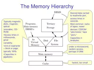
fig_04_31 Memory hierarchy fig_04_31
fig_04_32 Paging / Caching Why it typically works: locality of reference (spatial/temporal) “working set” Note: in real-time embedded systems, behavior may be atypical; but caching may still be a useful technique fig_04_32
fig_04_33 Typical memory system with cache: hit rate (miss rate) important fig_04_33
Basic caching strategies: Direct-mapped Associative Block-set associative questions: what is “associative memory”? what is overhead? what is efficiency (hit rate)? is bigger cache better? fig_04_33
Associative memory: storage location related to data stored Example—hashing: --When software program is compiled or assembled, a symbol table must be created to link addresses with symbolic names --table may be large; even binary search of names may be too slow --convert each name to a number associated with the name, this number will be the symbol table index For example, let a = 1, b = 2, c = 3,… Then “cab” has value 1 + 2 + 3 = 6 “ababab” has value 3 *(1 + 2) = 9 And “vvvvv” has value 5*22 = 110 Address will be modulo a prime p, if we expect about 50 unique identifiers, can take p = 101 (make storage about twice as large as number of items to be stored, reduce collisions) Now array of names in symbol table will look like: 0—> 1—> 2---> … 6--->cab … 9--->ababab--->vvvvv … Here there is one collision, at address 9; the two items are stored in a linked list Access time for an identifier <= (time to compute address) + 1 + length of longest linked list ~ constant
Caching: the basic process—note OVERHEAD for each task --program needs information M that is not in the CPU --cache is checked for M how do we know if M is in the cache? --hit: M is in cache and can be retrieved and used by CPU --miss: M is not in cache (M in RAM or in secondary memory) where is M? * M must be brought into cache * if there is room, M is copied into cache how do we know if there is room? * if there is no room, must overwrite some info M’ how do we select M’? ++ if M’ has not been modified, overwrite it how do we know if M’ has been modified? ++ if M’ has been modified, must save changes how do we save changes to M’?
Example: direct mapping 32-bit words, cache holds 64K words, in 128 0.5K blocks Memory addresses 32 bits Main memory 128M words; 2K pages, each holds 128 blocks (~ cache) fig_04_34 Tag table: 128 entries (one for each block in the cache). Contains: Tag: page block came from Valid bit: does this block contain data write-through: any change propagated immediately to main memory delayed write: since this data may change again soon, do not propagate change to main memory immediately—this saves overhead; instead, set the dirty bit Intermediate: use queue, update periodically When a new block is brought in, if the valid bit is true and the dirty bit is true, the old block must first be copied into main memory Replacement algorithm: none; each block only has one valid cache location fig_04_34 fig_04_35 fig_04_36 2 bits--byte; 9 bits--word address; 7 bits—block address (index); 11 (of 15)—tag (page block is from)
fig_04_37 Problem with direct mapping: two frequently used parts of code can be in different “Block0’s”—so repeated swapping would be necessary; this can degrade performance unacceptably, especially in realtime systems (similar to “thrashing” in operating system virtual memory system) Another method: associative mapping: put new block anywhere in the cache; now we need an algorithm to decide which block should be removed, if cache is full fig_04_37
fig_04_38 • Step 1: locate the desired block within the cache; must search tag table, linear search may be too slow; search all entries in parallel or use hashing • Step 2: if miss, decide which block to replace. • Add time accessed to tag table info, use temporal locality: • Least recently used (LRU)—a FIFO-type algorithm • Most recently used (MRU)—a LIFO-type algorithm • b. Choose a block at random fig_04_38 Drawbacks: long search times Complexity and cost of supporting logic Advantages: more flexibility in managing cache contents
Intermediate method: block-set associative cache Each index now specifies a set of blocks Main memory: divided into m blocks organized into n groups Group number = m mod n Cache set number ~ main memory group number Block from main memory group j can go into cache set j Search time is less, since search space is smaller How many blocks: simulation answer (one rule of thumb: doubling associativity ~ doubling cache size, > 4-way probably not efficient) fig_04_39 Two-way set-associative scheme fig_04_39
Example: 256K memory-64 groups, 512 blocks • Block Group (m mod 64) • 0 64 128 . . . 384 448 0 • 65 129 . . . 385 449 1 • 66 130 . . . 386 450 2 • . . . • 63 127 192 . . . 447 511 63
Dynamic memory allocation “virtual storage”): --for programs larger than main memory --for multiple processes in main memory --for multiple programs in main memory General strategies may not work well because of hard deadlines for real-time systems in embedded applications—general strategies are nondeterministic Simple setup: Can swap processes/programs And their contexts --Need storage (may be in firmware) --Need small swap time compared to run time --Need determinism Ex: chemical processing, thermal control fig_04_40 fig_04_40
fig_04_41 Overlays (“pre-virtual storage”): Seqment program into one main section and a set of overlays (kept in ROM?) Swap overlays Choose segmentation carefully to prevent thrashing fig_04_41
fig_04_42 Multiprogramming: similar to paging Fixed partition size: Can get memory fragmentation Example: If each partition is 2K and we have 3 jobs: J1 = 1.5K, J2 = 0.5K, J3 = 2.1K Allocate to successive partitions (4) J2 is using only 0.5 K J3 is using 2 partitions, one of size 0.1K If a new job of size 1K enters system, there is no place for it, even though there is actually enough unused memory for it fig_04_42 Variable size: Use a scheme like paging Include compaction Choose parameters carefully to prevent thrashing
fig_04_43 Memory testing: Components and basic architecture fig_04_43
Faults to test: data and address lines; stuck-at and bridging (if we assume no internal manufacturing defects) fig_04_45 fig_04_45
fig_04_49 ROM testing: stuck-at faults, bridging faults, correct data stored Method: CRC (cyclic reduncancy check) or signature analysis Use LFSR to compress a data stream into a K-bit pattern, similar to error checking (Q: how is error checking done?) ROM contents modeled as N*M-bit data stream, N= address size, M = word size fig_04_49
Error checking: simple examples • Detect one bit error: add a parity bit • Correct a 1-bit error: Hamming code Example: send m message bits + r parity bits The number of possible error positions is m + r + 1, we need 2r >= m + r + 1 If m = 8, need r = 4; ri checks parity of bits with i in binary representation Pattern: Bit #: 1 2 3 4 5 6 7 8 9 10 11 12 Info: r0 r1 m1 r2 m2 m3 m4 r3 m5 m6 m7 m8 --- --- 1 --- 1 0 0 --- 0 1 1 1 Set parity = 0 for each group r0: bits 1 + 3 + 5 + 7 + 9 + 11 = r0 + 1 + 1 + 0 + 0 + 1 r0 = 1 r1: bits 2 + 3 + 6 + 7 + 10 + 11 = r1 + 1 + 0 + 0 + 1 + 1 r1 = 1 r2: bits 4 + 5 + 6 + 7 + 12 = r2 + 1 + 0 + 1 r2 = 0 r3: bits 8 + 9 + 10 + 11 + 12 = r3 + 0 + 1 + 1 + 1 r3 = 1 Exercise: suppose message is sent and 1 bit is flipped in received message Compute the parity bits to see which bit is incorrect Addition: add an overall parity bit to end of message to also detect two errors Note: • this is just one example, a more general formulation of Hamming codes using the finite field arithmetic can also be given b. this is one example of how error correcting codes can be obtained, there are many more complex examples, e.g., Reed-Solomon codes used in CD players