Download
1 / 3
30 likes | 33 Views
The proliferation of thin wafer users and the high rate of portable device adoption<br>https://straitsresearch.com/report/thin-wafer-market/<br>

E N D
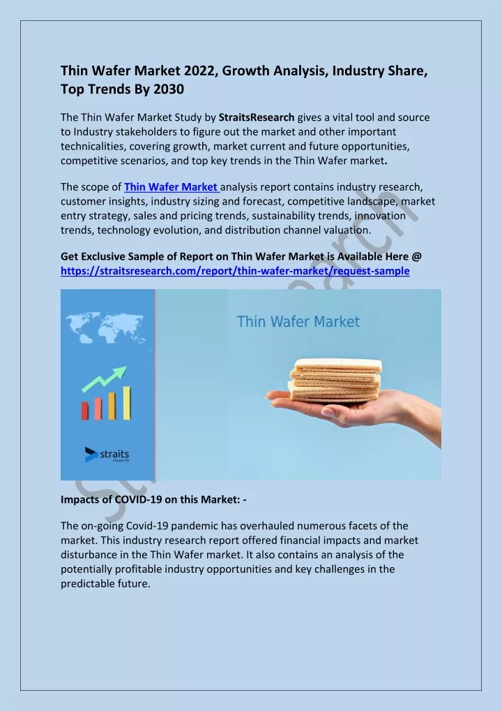
Thin Wafer Market 2022, Growth Analysis, Industry Share, Top Trends By 2030 The Thin Wafer Market Study by StraitsResearch gives a vital tool and source to Industry stakeholders to figure out the market and other important technicalities, covering growth, market current and future opportunities, competitive scenarios, and top key trends in the Thin Wafer market. The scope of Thin Wafer Market analysis report contains industry research, customer insights, industry sizing and forecast, competitive landscape, market entry strategy, sales and pricing trends, sustainability trends, innovation trends, technology evolution, and distribution channel valuation. Get Exclusive Sample of Report on Thin Wafer Market is Available Here @ https://straitsresearch.com/report/thin-wafer-market/request-sample Impacts of COVID-19 on this Market: - The on-going Covid-19 pandemic has overhauled numerous facets of the market. This industry research report offered financial impacts and market disturbance in the Thin Wafer market. It also contains an analysis of the potentially profitable industry opportunities and key challenges in the predictable future.
Competitive Landscape:- Major companies contributing in the global Thin Wafer market are GlobalWafers Co., Ltd, Shin-Etsu Chemical Co., My-Chip Production GmbH, EV Group, Siltronic AG, Polishing Corporation of America, Virginia Semiconductor Inc., ULVAC GmbH, Sil'tronix Silicon Technologies, Brewer Science, Inc., 3M Company, SK Siltron,among others. Geographic Analysis:- The global Thin Wafer market has been spread across North America, Europe, Asia-Pacific, the Middle East and Africa, and the Rest of the World. Do You Have Any Query Or Specific Requirements? Ask to Our Industry Expert @ https://straitsresearch.com/buy-now/thin-wafer-market/global/ Market Segmentation of Thin Wafer Market:- By Wafer Size: 125mm, 200mm, 300mm By Process: Temporary Bonding and Debonding, Carrier less/Taiko Process By Application: MEMS, CMOS Image Sensor, Memory, RF Devices, LED, Interposers, Logic, Others By Technology: Wafer Grinding, Wafer Polishing, Wafer Dicing Industry Drivers and Risks:- The report pays special attention to factors that underwrite to the Insurance Thin Wafer Market growth also called as market drivers. Any variations in these market dynamics directly affect the market growth hence the report offered a future insight into important key factors that should be observed and which could be leveraged by companies, vendors, industry distributors and all stakeholders alike to their advantage. The report also offers an insight into the key challenges faced by the market and the strategies used by existing industry players to overcome or avoid these risks. Click Here to Access the Full Report @ https://straitsresearch.com/report/thin-wafer-market
About Us: StraitsResearch.com is a leading market research and market intelligence organization, specializing in research, analytics, and advisory services along with providing business insights & market research reports. Contact Us: Email: sales@straitsresearch.com Address: 825 3rd Avenue, New York, NY, USA, 10022 Tel: +1 6464807505, +44 203 318 2846 Website: https://straitsresearch.com/