Download
1 / 23
330 likes | 776 Views
Binary Adder/Subtractor. Overflow. When does it occur? How do we detect it?. 01110 10000 + 5 0101 -4 1100 + 7 0111 -6 1010 +12 ? 01100 -10 ? 10110. Binary Multiplication. The binary digit multiplication table is trivial:

E N D
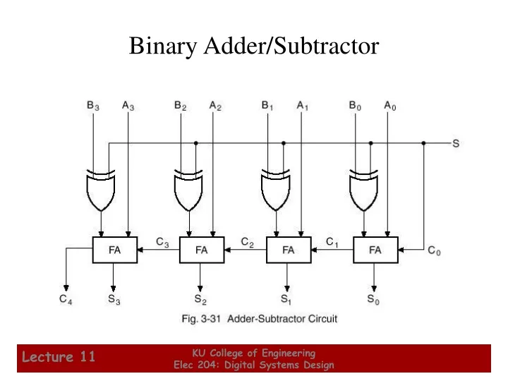
Binary Adder/Subtractor KU College of Engineering Elec 204: Digital Systems Design
Overflow • When does it occur? • How do we detect it? 01110 10000 + 5 0101 -4 1100 + 7 0111 -6 1010 +12 ? 01100 -10 ? 10110 KU College of Engineering Elec 204: Digital Systems Design
Binary Multiplication • The binary digit multiplication table is trivial: • This is simply the Boolean AND function. • Form larger products the same way we form larger products in base 10. (a × b) b = 0 b = 1 a = 0 0 0 a = 1 0 1 KU College of Engineering Elec 204: Digital Systems Design
2 3 7 × 1 4 9 2 1 3 3 9 4 8 - + 2 3 7 - - 3 5 3 1 3 Review - Decimal Example: (237 × 149)10 • Partial products are: 237 × 9, 237 × 40, and 237 × 100 • Note that the partial product summation for n digit, base 10 numbers requires adding up to n digits (with carries). • Note also n × m digit multiply generates up to an m + n digit result. KU College of Engineering Elec 204: Digital Systems Design
1 0 1 × 0 1 1 1 0 1 1 0 1 0 0 0 0 0 1 1 1 1 Example: (101 x 011) Base 2 • Partial products are: 101 × 1, 101 × 10, and 101 × 000 • Note that the partial productsummation for n digit, base 2numbers requires adding upto n digits (with carries) ina column. • Note also n× m digit multiply generates up to an m + n digit result (same as decimal). KU College of Engineering Elec 204: Digital Systems Design
Multiplier Boolean Equations • We can also make an n×m “block” multiplier and use that to form partial products. • Example: 2 × 2 – The logic equations for each partial-product binary digit are shown below: • We need to "add" the columns to getthe product bits P0, P1, P2, and P3. • Note that somecolumns maygenerate carries. b1 b0 ´ a1 a0 . . (a0 b1) (a0 b0) . . + (a1 b1) (a1 b0) P3 P2 P1 P0 KU College of Engineering Elec 204: Digital Systems Design
Multiplier Arrays Using Adders • An implementation of the 2 × 2 multiplier array is shown: KU College of Engineering Elec 204: Digital Systems Design
4-bit by 3-bit multiplier KU College of Engineering Elec 204: Digital Systems Design
Design by Contraction • Contraction is a technique for simplifying the logic in a functional block to implement a different function • The new function must be realizable from the original function by applying rudimentary functions to its inputs • Contraction is treated here only for application of 0s and 1s (not for X and X’) • After application of 0s and 1s, equations or the logic diagram are simplified KU College of Engineering Elec 204: Digital Systems Design
Design by Contraction Example: Increment • Contraction of a ripple carry adder to incrementer for n = 3 bits • Set B = 001 • The middle cell can be repeated to make an incrementer with n > 3. KU College of Engineering Elec 204: Digital Systems Design
Incrementing & Decrementing • Incrementing • Adding a fixed value to an arithmetic variable • Fixed value is often 1, called counting (up) • Examples: A + 1, B + 4 • Functional block is called incrementer • Decrementing • Subtracting a fixed value from an arithmetic variable • Fixed value is often 1, called counting (down) • Examples: A - 1, B - 4 • Functional block is called decrementer KU College of Engineering Elec 204: Digital Systems Design
Outputs Inputs Combina-tional Logic Storage Elements Next State State Introduction to Sequential Circuits • A Sequential circuit contains: • Storage elements:Latches or Flip-Flops • Combinatorial Logic: • Implements a multiple-output switching function • Inputsare signals from the outside. • Outputs are signals to the outside. • Other inputs, State orPresent State, are signals from storage elements. • The remaining outputs, Next State are inputs to storage elements. KU College of Engineering Elec 204: Digital Systems Design
Outputs Inputs Combina-tional Logic Storage Elements Next State State Introduction to Sequential Circuits • Combinatorial Logic • Next state functionNext State = f (Inputs, State) • Output function (Mealy)Outputs = g (Inputs, State) • Output function (Moore)Outputs = h (State) • Output function type depends on specification and affects the design significantly KU College of Engineering Elec 204: Digital Systems Design
Types of Sequential Circuits • Depends on the times at which: • storage elements observe their inputs, and • storage elements change their state • Synchronous • Behavior defined from knowledge of its signals at discrete instances of time • Storage elements observe inputs and can change state only in relation to a timing signal (clock pulses from a clock) • Asynchronous • Behavior defined from knowledge of inputs an any instant of time and the order in continuous time in which inputs change • If clock just regarded as another input, all circuits are asynchronous! • Nevertheless, the synchronous abstraction makes complex designs tractable! KU College of Engineering Elec 204: Digital Systems Design
Discrete Event Simulation • In order to understand the time behavior of a sequential circuit we use discrete event simulation. • Rules: • Gates modeled by anideal(instantaneous) function and a fixed gate delay • Any change in input values is evaluated to see if it causes a change in output value • Changes in output values are scheduled for the fixed gate delay after the input change • At the time for a scheduled output change, the output value is changed along with any inputs it drives KU College of Engineering Elec 204: Digital Systems Design
F(Instantaneous) A F DELAY 0.5 ns. B t (ns) A B F(I) F Comment – 1 1 0 0 A=B=1 for a long time Þ Ü 0 1 0 F(I) changes to 1 1 0 1 0 Ü 0 1 1 F changes to 1 after a 0.5 ns delay 1 0 0.5 Ü Þ 1 1 F(Instantaneous) changes to 0 0.8 1 0 1 0 Þ 0.13 1 1 0 F changes to 0 after a 0.5 ns delay 1 0 Simulated NAND Gate • Example: A 2-Input NAND gate with a 0.5 ns. delay: • Assume A and B have been 1 for a long time • At time t=0, A changes to a 0 at t= 0.8 ns, back to 1. KU College of Engineering Elec 204: Digital Systems Design
0.2 0.5 0.4 Gate Delay Models • Suppose gates with delay n ns are represented for n = 0.2 ns, n = 0.4 ns,n = 0.5 ns, respectively: KU College of Engineering Elec 204: Digital Systems Design
0.2 0.5 0.4 0.4 A B S S Y Circuit Delay Model A • Consider a simple 2-input multiplexer: • With function: • Y = A for S = 0 • Y = B for S = 1 • “Glitch” is due to delay of inverter Y S B KU College of Engineering Elec 204: Digital Systems Design
S Y B 0.2 0.5 0.4 0.4 S S Y Storing State • What if A con-nected to Y? • Circuit becomes: • With function: • Y = B for S = 1, andY(t) dependent onY(t – 0.9) for S = 0 • The simple combinational circuit has now become a sequential circuit because its output is a function of a time sequence of input signals! B Y is stored value in shaded area KU College of Engineering Elec 204: Digital Systems Design
B S Y Comment 1 0 0 Y “remembers” 0 Y = B when S = 1 1 1 1 1 0 1 Now Y “remembers” B = 1 for S = 0 0 0 1 No change in Y when B changes Y = B when S = 1 0 1 0 0 0 0 Y “remembers” B = 0 for S = 0 No change in Y when B changes 1 0 0 Storing State (Continued) • Simulation example as input signals change with time. Changes occur every 100 ns, so that the tenths of ns delays are negligible. • Y represent the state of the circuit, not just an output. Time KU College of Engineering Elec 204: Digital Systems Design
S Y B 0.2 0.2 0.5 0.4 0.4 Comment B S Y 0 1 0 Y = B when S = 1 1 1 1 1 0 1 Now Y “remembers” A 1.1 ns later 1 0 0 Y, Y, 1.1 ns later 1 0 1 Y, 1.1 ns later 1 0 0 Storing State (Continued) • Suppose we placean inverter in the“feedback path.” • The following behavior results: • The circuit is saidto be unstable. • For S = 0, thecircuit has becomewhat is called anoscillator. Can be used as crude clock. KU College of Engineering Elec 204: Digital Systems Design
Q R S Q Q Comment 1 1 ? ? Stored state unknown 1 0 1 0 “Set” Q to 1 1 1 1 0 Now Q “remembers” 1 0 1 0 1 “Reset” Q to 0 Basic (NAND) S – R Latch S (set) Q • “Cross-Coupling” two NAND gates gives the S -R Latch: • Which has the time sequence behavior: • S = 0, R = 0 is forbidden as input pattern R (reset) Time 1 1 0 1 Now Q “remembers” 0 0 0 1 1 Both go high 1 1 ? ? Unstable! KU College of Engineering Elec 204: Digital Systems Design
R (reset) Q Q S (set) Time R S Q Q Comment 0 0 ? ? Stored state unknown 0 1 1 0 “Set” Q to 1 0 0 1 0 Now Q “remembers” 1 1 0 0 1 “Reset” Q to 0 0 0 0 1 Now Q “remembers” 0 1 1 0 0 Both go low 0 0 ? ? Unstable! Basic (NOR) S –R Latch • Cross-coupling twoNOR gates gives theS – R Latch: • Which has the time sequence behavior: KU College of Engineering Elec 204: Digital Systems Design