Download
1 / 6
80 likes | 100 Views
Explore the microfabrication of 100 GHz test structures on Corning glass cover slips, designed for optimal frequency response around 100 GHz. Learn about the substrate choice, dimensions calculation, and fabrication process with exact geometry details.

E N D
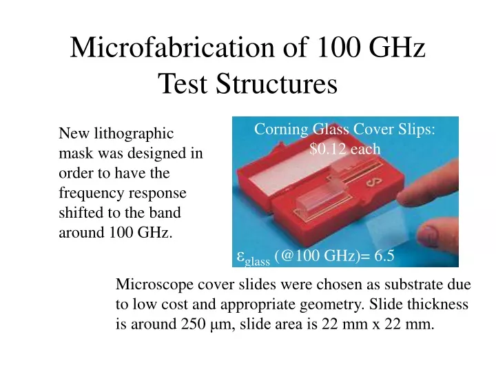
Microfabrication of 100 GHz Test Structures Corning Glass Cover Slips: $0.12 each New lithographic mask was designed in order to have the frequency response shifted to the band around 100 GHz. εglass (@100 GHz)= 6.5 Microscope cover slides were chosen as substrate due to low cost and appropriate geometry. Slide thickness is around 250 μm, slide area is 22 mm x 22 mm.
Exact Geometry of Features on the 100 GHz Mask • The following dimensions were calculated using: • Target frequency: 100 GHz. • Previous design (12 GHz) dimensions. • Substrate relative permittivity (6.5) at target frequency.
Array area: 15 mm x 15 mm Array: 33 x 33 Alignment - 1: Array to Glass (during Fabrication) Alignment - 2: Glass to Glass (Stacking) (during Measurement)
Fabricated Structures • Fabrication at Microelectronics Facility of FORTH, Heraklion. • With Dr. George Konstantinidis. • Method: Image Reversal Lithography(AZ5214) / E-Gun Metal Deposition (5000Å Ag) / Lift-Off