Download
1 / 21
210 likes | 232 Views
Conducted at CERN in 2006, the experiment tested crystal collimation for LHC particles. Walter Scandale led the study on silicon crystal techniques, volume reflections, and channeling efficiencies with impressive results. The study showcased efficient deflection of halo particles and selective scattering processes. With future plans for crystal workshops and advancements in crystal installations at FNAL, the experiment opens new possibilities in high-energy physics research.

E N D
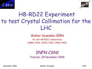
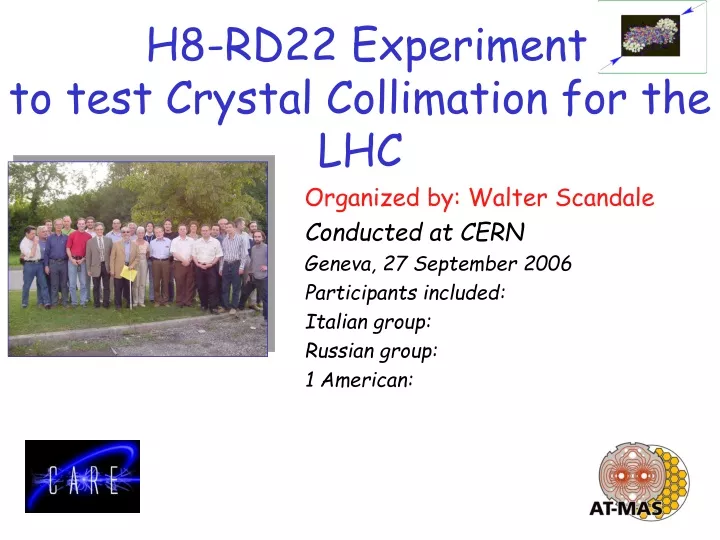
Organized by: Walter Scandale Conducted at CERN Geneva, 27 September 2006 Participants included: Italian group: Russian group: 1 American: H8-RD22 Experimentto test Crystal Collimation for the LHC
Particles are channeled Lattice of crystal. Volume Capture: Volume reflections from atomic planes 980-GEV BEAM CHANNELING Independent simulations by V. Biryukov and Y. Ivanov show channeling efficiencies of 90% to 95% possible.
Walter Scandale Amorphous scatterer Crystal channeling: a smart approach for primary collimation • A bent crystal should efficiently deflect halo particles away from the beam core toward a downstream massive absorber • The selective and coherent scattering on atomic planes of an aligned Si-crystal replaces the random scattering process on single atoms of an amorphous target
Walter Scandale Silicon crystals Strip Crystals have been fabricated in theSensors and Semiconductor Laboratory (Ferrara, Italy) Crystal sizes: ~ 0.9 x 70 x 3 mm3 Quasi-Mosaic Crystals have been fabricated in PNPI (Gatchina, Russia) Crystal plate sizes: ~ 1 x 30 x 55 mm3 critical angle for 400 GeV/c protons ≈ 10 μrad
Walter Scandale S1 Layout scheme (not to scale) Goniometer with crystal holders • Scintillators (S1-S6) • Scintillating Hodoscope (H) S3 GC S5 vacuum BM BM vacuum p H S6 S2 S4 Si microstrips (AMS) Si microstrips (AGILE) 70 m • Gas Chamber (GC) • Bending Magnet (BM)
Walter Scandale VR VC Volume reflection (110) Si crystal – simulation results H8 microbeam – 400 GeV protons, divergence – 3 μrad Crystal bending angle α=100 μrad, length S=1 mm Angular distribution Volume reflection angle θVR = 14.3 μrad , σ=5.1 μrad Volume reflected fraction with θ<0,VR– 96% Volume captured fraction at the exit from the crystal, VC – about 1.5%
Walter Scandale 0 Ch Channeling (110) Si crystal – simulation results H8 microbeam – 400 GeV protons, divergence – 3 μrad Crystal bending angle α=100 μrad, length S=1 mm Angular distribution Deflection efficiencyof channeled fraction – 80% Full width of deflected fraction – 20 μrad Reduction of channeled fraction due to multiple scattering – about 6%
Walter Scandale Scan of Strip Crystal (1) (mm) Orientation (111) Bending angle: ~ 200 microrad Crystal sizes: 0.5 × 70 × 1.85 mm3
Walter Scandale Scan of Strip Crystal (1) measured volume reflection angle: ~ 10 μrad
Walter Scandale Scan of Strip Crystal (2) Orientation (110) Crystal sizes: 0.9 × 70 × 3 mm3
Walter Scandale Scan of Quasi-Mosaic Crystal (1) Orientation (111) Bending angle: ~ 80 microrad Crystal sizes: 30 × 58 × 0.84 mm3 measured volume reflection angle: ~ 10 μrad
Walter Scandale Double Reflection on Quasi-Mosaic Crystals (1) double reflection angle: ~ 20 μrad
Walter Scandale Double Reflection on Quasi-Mosaic Crystals (2) Two crystals displaced by 1 mm: not perfect alignment
Walter Scandale Conclusive remarks • First observation of Volume Reflection Effect in bent silicon crystals with 400 GeV/c protons with efficiency close to unity • Measurement of volume reflection angle: ~ 10 μrad • First observation of Double Reflection using two crystals in series: combined reflection angle is ~ 20 μrad and efficiency close to 1 • Channeling and Volume Reflection phenomena studied with Strip and Quasi-Mosaic Silicon Crystals (different fabrication techniques) • Measurement of crystals with different crystalline planes orientations: (111) and (110)
Future Plans • There was talk of a crystal workshop in a couple of months to propose experiments in the Tevatron and/or SPS to collimate channeled and volume reflected beams to be conducted spring 2007. • We are proceeding with installing the crystal FNAL has but have many problems with inchworm drive.
Walter Scandale The beam Beam parameters • Primary 400 GeV/c proton beam • Typical beam intensity at T4 target: ~ 20 1011 ppp • The experiment requires reduced rates < 104-5 ppp (for silicon detectors DAQ) Beam measurements • ~ 10 μrad divergence • ~ 1 mm (r.m.s.) beam dimension at 65 m with not aligned crystal Crystal not aligned 1 ch = 0.110 mm
Walter Scandale Crystals High precision goniometric system Silicon detector Scintillator Goniometer Granite Block
Walter Scandale AMS Silicon Detectors Silicon thickness: 300 μm Detector upstream of the crystal (on the granite block): • 1 double-sided silicon microstrip detector: - Resolution ~ 10 μmin bending direction (X coordinate) - Resolution ~ 30 μmin non-bending direction (Y coordinate) - Active area ~ 7.0 x 2.8 cm2 Detector downstream of the crystal (on the granite block) : • 1 BABY double-sided microstrip detectors (IRST): • Resolution better than 10 μmin bending direction • Resolution better than 20 μmin non-bending direction • Active area ~ 1.9 x 1.9 cm2 DOWNSTREAM TELESCOPE (at 65 m from crystal location): • 4 AMS LADDERS: • Resolution ~ 10 μmin bending direction • Resolution ~ 30 μmin non-bending direction • Active area ~ 4 x 7 cm2
Walter Scandale AGILE Silicon Detectors • Single-sided silicon strip detectors • Built by Agile (INFN/TC-01/006) • active area 9.5×9.5 cm2 • Spatial resolution: ~ 40 m at normal incidence (~ 30 m for tracks at 11°) • Silicon thickness: 410 μm • Upstream detector (before goniometer): • 2 silicon detectors at 90° (corresponds to 1 X-Y plane) • Downstream detector 1 (at 65 m from crystal location): • 4 X-Y silicon planes • Downstream detector 2 (at 65 m from crystal location): • 6 X-Y silicon planes interleaved with 300 mtungsten planes
Walter Scandale Scintillators and trigger system • SCINTILLATING DETECTORS: • finger scintillators (S1,S5): 0.1 × 1 × 10 mm3 (S1,S5): and 0.05 × 1 × 10 mm3 (S2) to choose a narrow beam fraction • 1 finger scintillator (S6): 2 × 1 × 10 mm3 • scintillating Hodoscope (H): 16 strips with 3.2 × 3.0 cm2 sensitive area (each strip is 2 × 4 × 40 mm3) read-out by 16 ch. MAPMT (fast beam monitoring) • 2 scintillator plates (S3,S4): 100 × 100 × 4 mm3 used for triggering the silicon detectors • SCINTILLATORS ELECTRONICS and TRIGGER: • programmable Trigger Logic Unit (high flexibility: many trigger conditions possible)