Download
1 / 8
80 likes | 325 Views
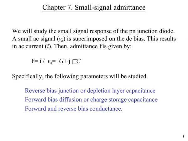
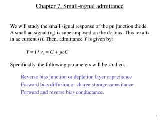
Chapter 7. Small-signal admittance. We will study the small signal response of the pn junction diode. A small ac signal ( v a ) is superimposed on the DC bias. This results in ac current ( i ). Then, admittance Y is given by: Y = i / v a = G + j C

E N D
Chapter 7. Small-signal admittance We will study the small signal response of the pn junction diode. A small ac signal (va) is superimposed on the DC bias. This results in ac current (i). Then, admittance Y is given by: Y = i/va = G + jC Specifically, the following parameters will be studied: • Reverse bias junction or depletion layer capacitance • Forward bias diffusion or charge storage capacitance • Forward and reverse bias conductance.
Capacitance measurements I = DC i = ac Y = admittance i and va depend on the applied DC bias Model for a diode under ac
Reverse bias junction capacitance A pn junction under reverse bias behaves like a capacitor. Such capacitors are used in ICs as voltage-controlled capacitors. Depletion layer width under small ac superimposed on DC bias voltage. Looks similar to a parallel plate capacitor. where W is the depletion-layer width under DC bias.
Reverse bias junction capacitance For pn junction For p+n or pn+ junction where NB is the doping on the lightly doped side For asymmetrically doped junction CJ increases with NB1/2 CJ decreases with applied reverse bias
Parameter extraction/profiling C-V data from a pn junction is routinely used to determine the doping profile on the lightly doped side of the junction. 2 1/Cj2 [F–2 ] 1 If the doping on the lightly doped side is uniform, a plot of 1/CJ2 versus VA should be a straight line with a slope inversely proportional to NB and an extrapolated 1/CJ2 = 0 intercept equal to Vbi. 0 –10 –5 0 VA [Volts] Intercept = Vbi
Forward bias diffusion capacitance, CD CD isalso called the charge storage capacitance. The variation of the injected minority-carrier charge, which is a function of the applied bias, results in the diffusion capacitance. Both CJ and CD are always present, but for the forward-bias case, CD becomes dominant. n-type p-type Origin of diffusion capacitance pn0 np0 x For a p+n junction, I = Qp/p where Qp is total excess charge in n-side
CJ Rs CD GD Forward bias conductance Assumes Complicated at higher frequencies. VApplied = VA Equivalent circuit for a diode VJ
Example Problem: Consider a p+n junction forward biased such that the forward current is 1 mA. Assume the lifetime of holes is 10–7 s. Calculate the diffusion capacitance and the diffusion resistance. Solution: CD = 3.86 nF rd = 1/GD = 25.9 The current through the depletion layer will mostly be carried by (holes, electrons: choose one)? Plot the current carried by the holes and electrons through the n-type region, assuming that the diffusion length of holes is 1m.