Download
1 / 13
130 likes | 413 Views
Using GaP Avalanche Photodiodes for Photon Detection. Abigail Lubow EE Senior Project Fall 2001 and Spring 2002 Advisor: Professor Woodall. Pictures from http://www.roithner-laser.com/UV-PD.html. Background. Avalanche photodiodes (APDs) are high gain photodetectors.

E N D
Using GaP Avalanche Photodiodes for Photon Detection Abigail Lubow EE Senior Project Fall 2001 and Spring 2002 Advisor: Professor Woodall Pictures from http://www.roithner-laser.com/UV-PD.html
Background • Avalanche photodiodes (APDs) are high gain photodetectors. • Nonavalanching p-n and p-i-n photodetectors have unity gain. By contrast, APDs use the avalanching process to produce a higher gain. • This device addresses the need for solar blind UV detectors. • Potential applications: High density optical storage and detection of tryptophan flourescence (348nm). • This project is the first time GaP has been used to create an APD.
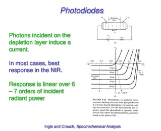
Photodiodes Figure 1. • Incident photons are absorbed in the photodiode giving rise to electron-hole pairs. • Gain = 1. Impact ionization will increase the gain above 1.
Impact Ionization • Definition: “a snowballing creation of carriers very similar to an avalanche of snow on a mountain side.”from Pierret’s Semiconductor Device Fundamentals • Conditions: Applied voltage (VA) is negative and VA Vbreakdown. Figure 2.
Why use GaP? • It is more commonly available and less expensive than other wide bandgap materials such as SiC and GaN. • For GaP, ni 1 /cm3 and for Si, ni = 1 x 10¹⁰/cm3. GaP p-n junction will have a smaller reverse current: • Large bandgaps correspond to small wavelengths: Eph = 1.24/. GaP bandgap = 2.26 eV, Si bandgap = 1.12 eV Figure 3.
p-GaP, Be doped grading from 210^18 to 210^19 (surface) over 3000A I- GaP, 3000 A n-GaP, 210^18, 5000 A Semi-insulating super lattice buffer n-GaP substrate P-I-N GaP Sample Figure 4. Figure 5. • Fig. 4. P-I-N structure: Electric field in graded p-layer separates electrons and holes. • Fig. 5. Electrochemical CV measurement. “+” for n type and “o” for p type.
Measurements: Current vs. Voltage Figure 6. Avalanching occurs at about -20V. Dark current is 1 × 10-¹³ A.
Measurements: Quantum efficiency vs. wavelength Figure 7. QE is “the ratio of the number of carriers generated to the number of photons incident upon the active region.”www.seas.gwu.edu/~ecelabs/appnotes/PDF/LED/LEDterms.pdf
Surface Band Bending Figure 8. • Surface band bending due to the “Fermi level pinning.” • Electron loss due to the surface recombination.
Measurements: Gain vs. Voltage Figure 9. • Gain results from the impact ionization process. • Large gains start at –20V for UV and white light. • Gains reach as high as 1000.
Measurements: Photocurrent vs. Wavelength Figure 10. • Current decreases at small wavelengths due to surface pinning. • Current decreases at large wavelengths due to low absorption coefficients.
Metal 0.25 m I-GaP 50 nm p-GaP doped 1*10^18cm^-3 Be 0.1 m I-GaP 1.0 m n-GaP doped 5*10^18 cm^-3 Si GaP n+ Substrate Schottky Device Figure 11. • SAM structure Schottky device improves absorption efficiency and reduces noise. • Processing Issue: Choice of metal with low light loss
Summary • GaP APD has been chosen for use as a solar blind UV detector. • P-I-N device showed promising performance with high gain, low dark current, and high QE at medium wavelengths. • UV QE needed improvement. A Schottky device structure was proposed.