Download
1 / 47
470 likes | 488 Views
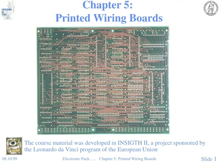
Chapter 5: Printed Wiring Boards. The course material was developed in INSIGTH II, a project sponsored by the Leonardo da Vinci program of the European Union. Substrate. The purpose of the substrate for electronic component mounting is: Mechanical support Electrical interconnection

E N D
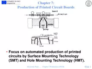
Chapter 5: Printed Wiring Boards The course material was developed in INSIGTH II, a project sponsored by the Leonardo da Vinci program of the European Union Electronic Pack….. Chapter 5: Printed Wiring Boards
Substrate • The purpose of the substrate for electronic component mounting is: • Mechanical support • Electrical interconnection • Heat conduction Electronic Pack….. Chapter 5: Printed Wiring Boards
Organic Substrate: Printed Wiring Boards (PWB) • Requirements: • Electrical properties • Mechanical properties • Chemical resistance • Fire resistance • Process ability • Adhesion • Low moisture absorption Fig. 5.1: Woven glass fibre for printed wiring board reinforcement Electronic Pack….. Chapter 5: Printed Wiring Boards
Printed Wiring Boards, continued Table 5.1: Conventional laminates for printed wiring boards. (The designations are according to National Electrical Manufacturers Association, NEMA, USA.) Electronic Pack….. Chapter 5: Printed Wiring Boards
Printed Wiring Boards, continued Fig. 5.2: Printed wiring board structures with varying complexity:a) Single sided and double sided.b) Double sided through hole plated with bare Cu or Sn/Pb surface.c) Four layer board.d) Six layer board with two Cu/Invar/Cu cores. Electronic Pack….. Chapter 5: Printed Wiring Boards
Printed Wiring Boards, continued Generation of Design Data, Photo- or Laser Plotting Fig. 5.3: Photo plotter, schematically. Electronic Pack….. Chapter 5: Printed Wiring Boards
Single Sided Boards • 1. Drilling / punching of registration holes • 2. Panel cleaning • 3. Printing of etch resist • 4. Etching • 5. Stripping • 6. Printing solder resist • 7. Curing of solder resist • 8. Cleaning of solder areas • 9. Deposition of solder coating • 10. Punching of holes and edge contour (or drilling/milling)This is a subtractive process • Alternative: Additive processes Electronic Pack….. Chapter 5: Printed Wiring Boards
Single Sided Boards, continued Fig. 5.4: Process steps of "print and etch" process for single sided boards Electronic Pack….. Chapter 5: Printed Wiring Boards
Double Sided ThroughHole Plated Boards • 1. Drilling • 2. Cleaning of the surfaces and hole ("deburring"), and a mild etch to ensure adhesion in later steps • 3. Activation for chemical plating. • Dipped into a solution containing Sn2+ ions, to increase the sensitivity of the surface. The activation takes place in an acidic solution of palladium chloride, that is transformed into metallic Pd. Reaction: Sn2+ + Pd2+ -> Sn4+ + Pd.In the later plating process, Pd catalyses the deposition of copper. Electronic Pack….. Chapter 5: Printed Wiring Boards
Double Sided ThroughHole Plated Boards, cont • 4. Chemical plating of Cu: • Dipped into a reducing bath containing Cu2+ ions, for example in the form of dissolved CuSO4. • Formaldehyde, HCHO, is the common means of reduction. In this bath, Cu2+ is reduced to Cu that covers the whole surface, including the holes, also where the surface is electrically insulating. At the same time formaldehyde is oxidised into acetic acid. • The plated thickness is approximately 3 µm. The purpose is to create an electrically conducting surface everywhere, for the subsequent step. • 5. Electrolytic plating of Cu: • dipped into an electrolyte that contains Cu2+ ions, such as CuSO4 dissolved in H2SO4. The panel forms the negative electrode (cathode), and a metallic copper plate forms the positive electrode (anode) of an electrolytic cell. At the anode copper is dissolved: • Cu -> Cu2+ + 2e-. • The reaction at the cathode is the following: • Cu2+ + 2e- -> Cu, • thus, metallic copper is deposited on the panel. Approximately 25 – 30 µm Cu is normally plated, in order to get good coverage in the via holes. Electronic Pack….. Chapter 5: Printed Wiring Boards
Double Sided ThroughHole Plated Boards, cont • 6. Pattern definition • Dry film photoresist is laminated on to both sides, normally negative resist. The resist is illuminated through a positive photographic mask and is developed. The pattern is therefore black on the photomask, and the photoresist will dissolve where there is a pattern, during the development. • 7. Tin/lead plating for etch masking: • The panel is connected to the cathode of an electrolytic bath containing Sn2+ and Pb2+ ions. The anode is metallic Sn/Pb alloy. The electrolyte is based on fluoroboric acid, HBF4. The ratio between the concentration of the ions in the bath and on the anode, is such that the deposited layer of metal on the panel will be approximately the eutectic mixture 63Sn/37Pb (percent by weight). The normal thickness is about 7 µm. After this the photoresist is dissolved in a suitable solvent, for instance methylene chloride. Electronic Pack….. Chapter 5: Printed Wiring Boards
Double Sided ThroughHole Plated Boards, cont • 8. Etching: • The Cu foil is etched simultaneously on both sides, analogous to step 4, Section 5.5, but with an ammonia-based etch bath, which does not attack Sn/Pb. The plated Sn/Pb serves as an etch resist. After the etching, the Cu is covered with Sn/Pb where we want conductor pattern and solder lands, as well as in the holes through the board. • 9. Fusing: • If it is desired to have Sn/Pb on the completed board, a "fusing" step follows. It consists in heating of the board to a temperature where the alloy melts and changes its crystalline structure. It flows and covers the nearly vertical edges of the etched copper. We get an intermetallic copper/tin interfacing layer. The heating may take place in hot air or oil, by IR radiation heating, etc. • 10. Organic solder resist may be added by screen printing Electronic Pack….. Chapter 5: Printed Wiring Boards
Double Sided Through Hole Plated Boards, cont Fig. 5.5: Through hole plated PWB, process steps: a) Panel plating. b) Pattern plating. c) Hot air levelling. Electronic Pack….. Chapter 5: Printed Wiring Boards
Double Sided Through Hole Plated Boards:Choice of Surface Metallisation and Solder Resist Fig. 5.6.a: Selective Sn/Pb surface coverage with hot air levelling. The alternatives, bare Cu or Sn/Pb on all Cu surface, are shown in Figure 5.2 b). Electronic Pack….. Chapter 5: Printed Wiring Boards
Choice of Surface Metallisation and Solder Resist, continued Fig. 5.6.b: "Tenting", i.e. covering of the via holes by dry film solder resist. Electronic Pack….. Chapter 5: Printed Wiring Boards
Multilayer Printed Wiring Boards • 1. Drilling • 2. Rinse, Photo process for inner layers • 3. Etch inner layers • 4. Black oxidation for adhesion promotion • 5. Baking • 6. Lamination • 7. Drilling of through holesFurther process as for double layer boards Electronic Pack….. Chapter 5: Printed Wiring Boards
Multilayer Printed WiringBoards, continued Fig. 5.7: Process steps for multilayer printed wiring boards with holes only through the board. Electronic Pack….. Chapter 5: Printed Wiring Boards
Multilayer PrintedWiring Boards, continued Fig. 5.8: Types of via holes: a) Through hole. b) Buried hole. c) Blind hole. Figure d) shows a microscope section of a drilled blind via. (Contrave´s "Denstrate" process). Electronic Pack….. Chapter 5: Printed Wiring Boards
Fine Line PrintedWiring Boards, Additive Process Fig. 5.9 a): The development of minimum line width from 1965 until 1990. The figures in the ovals tell how many conductors can be positioned between the leads of DIP-components with a lead pitch of 0.1" (number of "channels"). Electronic Pack….. Chapter 5: Printed Wiring Boards
Fine Line PrintedWiring Boards, Additive Process, continued • Etch control: Under etch/etch factor • Additive process • Clean-room • Collimated light Fig. 5.9 b): Underetch and etch factor. Electronic Pack….. Chapter 5: Printed Wiring Boards
Fine Line Printed Wiring Boards: Photolithographic Process Fig. 5.10.a: Machine for double sided illumination with parallel light, for pattern transfer from photographic film for fine line printed wiring boards. Electronic Pack….. Chapter 5: Printed Wiring Boards
Fine Line Printed Wiring Boards: Photolithographic Process, continued Fig. 5.10.b : Automatic in-line system for lamination of photoresist, illumination and development, in an enclosed clean room atmosphere. Electronic Pack….. Chapter 5: Printed Wiring Boards
Metal Core Printed Wiring Boards • Better heat conduction • TCE matching with ceramic packages • Most common: Cu/Invar/Cu Fig. 5.2.d) Six layer board with two Cu/Invar/Cu cores. Electronic Pack….. Chapter 5: Printed Wiring Boards
Metal Core Boards, continued Fig. 5.12 a): Cross section of metal core board with one Cu/Invar/Cu core (Texas Instruments). Fig. 5.12 b):Thermal coefficient of expansion of Cu/Invar/Cu, as function of the composition (Texas Instruments). Electronic Pack….. Chapter 5: Printed Wiring Boards
New Materials for PWBs • Higher Tg • Better dimensional stability • er low, not dependent on T, f, or moisture • Low losses • Lower TCE • Purpose • High frequency use • Controlled characteristic impedance • High reliability • Materials • Cyanate ester • PTFE (Teflon) • Polyimide • and others Electronic Pack….. Chapter 5: Printed Wiring Boards
New Materials for PWBs,continued Fig. 5.13: TCE for FR-4 below and above Tg in a): the x or y direction, b): the z-direction. Electronic Pack….. Chapter 5: Printed Wiring Boards
New Materials for PWBs,continued Table 5.2: Material parameters for polymers for printed wiring boards Electronic Pack….. Chapter 5: Printed Wiring Boards
New Materials for PWBs,continued Fig. 5.14: Frequency dependence of er and tan d for FR-4. er :Relative dielectric constant. tan d: Loss tangent. Electronic Pack….. Chapter 5: Printed Wiring Boards
Commercial Products Table 5.3: Materials parameters for important materials combinations and some commercial products for high performance printed wiring boards. Electronic Pack….. Chapter 5: Printed Wiring Boards
Commercial Products,continued Fig. 5.15 a): Structure of Rogers material RO2800. Electronic Pack….. Chapter 5: Printed Wiring Boards
Commercial Products,continued Fig. 5.15 b): Combination of Gore-Ply and FR-4 gives a simple process, and at the same time low dielectric losses and reduced capacitance to ground. Electronic Pack….. Chapter 5: Printed Wiring Boards
Commercial Products,continued Fig. 5.16: Attenuation in (dB) as function of frequency for a one meter long stripline, for the high performance materials Gore, Nelco and polyimide, compared to FR-4. Electronic Pack….. Chapter 5: Printed Wiring Boards
Commercial Products,continued Fig. 5.17: Top: Microwire from PCK, with conductors insulated with organic insulation, and a metal foil as ground plane. Bottom: Next generation technology, where each conductor has its own metal shield. Electronic Pack….. Chapter 5: Printed Wiring Boards
Commercial Products, continued Fig. 5.18: The equipment head that deposits the conductors on the laminate for Microwire. Electronic Pack….. Chapter 5: Printed Wiring Boards
Special Boards • Flexible printed wiring boards • Dynamic or static bending. • Uses: Movable parts and odd shaped, cramped places Electronic Pack….. Chapter 5: Printed Wiring Boards
Flexible PrintedWiring Boards, continued Fig. 5.19: Flexible printed wiring boards: Most of the electronics in Minoltas camera Maxxum 9000 is on two flexible printed circuit boards. Electronic Pack….. Chapter 5: Printed Wiring Boards
Flexible PrintedWiring Boards, continued Table 5.4: Properties for materials used for flexible printed wiring boards. Electronic Pack….. Chapter 5: Printed Wiring Boards
Flexible PrintedWiring Boards, continued Fig. 5.20: Cross section of flexible PWB: Top: Single layer conductor foil. Bottom: Double layer conductors with through hole plating. Electronic Pack….. Chapter 5: Printed Wiring Boards
Membrane Switch Panels Purpose: Switches and informative instrument fronts. Fig. 5.21 a): Membrane switch panel, schematically. Top: Structure Bottom: Cross section of a normal panel and a panel with metal dome. Electronic Pack….. Chapter 5: Printed Wiring Boards
Membrane Switch Panels, continued Fig. 5.21 b): Exploded view of simple switch panel Electronic Pack….. Chapter 5: Printed Wiring Boards
3 D Moulded Boards • Combine substrate and chassis, integrated stand-offs, etc. • Materials: • Polysulphone, polyetherimide, etc. Electronic Pack….. Chapter 5: Printed Wiring Boards
3 D Moulded Boards, continued Table 5.5: Materials used for moulded circuit boards, and their properties, compared to epoxy and polyimide. Electronic Pack….. Chapter 5: Printed Wiring Boards
3 D Moulded Boards, continued Fig. 5.22.a: 3 dimensional moulded component carrier in a telephone application. Electronic Pack….. Chapter 5: Printed Wiring Boards
3 D Moulded Boards, continued Fig. 5.22.b: 3 dimensional moulded component carrier in a power supply application. Electronic Pack….. Chapter 5: Printed Wiring Boards
3 D Moulded Boards, continued Fig. 5.23: The process for moulding of a 3-dimensional substrate with Cu conductor patterns deposited on a temporary film. Electronic Pack….. Chapter 5: Printed Wiring Boards
3 D Moulded Boards, continued Fig. 5.24: Two steps moulding process for preparation for chemical plating of the conductor pattern on 3-D component substrates. The first moulding is done with a catalytically activated plastic, the second with "passive" plastic, where chemical plating is not sticking. (PCK, USA). Electronic Pack….. Chapter 5: Printed Wiring Boards
End of Chapter 5: Printed Wiring Boards • Important issues: • When…. • Questions and discussions? Electronic Pack….. Chapter 5: Printed Wiring Boards