Download
1 / 6
60 likes | 200 Views
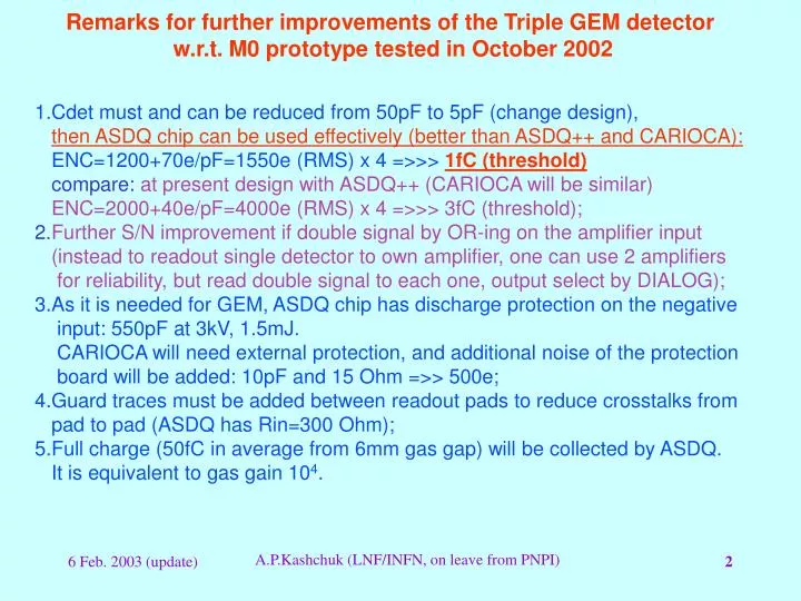
Remarks for further improvements of the Triple GEM detector w.r.t. M0 prototype tested in October 2002. 1.Cdet must and can be reduced from 50pF to 5pF (change design), then ASDQ chip can be used effectively (better than ASDQ++ and CARIOCA):

E N D
Remarks for further improvements of the Triple GEM detector w.r.t. M0 prototype tested in October 2002 1.Cdet must and can be reduced from 50pF to 5pF (change design), then ASDQ chip can be used effectively (better than ASDQ++ and CARIOCA): ENC=1200+70e/pF=1550e (RMS) x 4 =>>>1fC (threshold) compare: at present design with ASDQ++ (CARIOCA will be similar) ENC=2000+40e/pF=4000e (RMS) x 4 =>>> 3fC (threshold); 2.Further S/N improvement if double signal by OR-ing on the amplifier input (instead to readout single detector to own amplifier, one can use 2 amplifiers for reliability, but read double signal to each one, output select by DIALOG); 3.As it is needed for GEM, ASDQ chip has discharge protection on the negative input: 550pF at 3kV, 1.5mJ. CARIOCA will need external protection, and additional noise of the protection board will be added: 10pF and 15 Ohm =>> 500e; 4.Guard traces must be added between readout pads to reduce crosstalks from pad to pad (ASDQ has Rin=300 Ohm); 5.Full charge (50fC in average from 6mm gas gap) will be collected by ASDQ. It is equivalent to gas gain 104. A.P.Kashchuk (LNF/INFN, on leave from PNPI)
Where this ‘blocking’ capacitor? Double signal A.P.Kashchuk (LNF/INFN, on leave from PNPI)
‘Blocking’ capacitor(defines the current return path) Cathode Drift gap GEM1 Transfer1 GEM2 Transfer2 in chain GEM3 Induction gap Anode To be cancelled or minimized To be maximized Add 1000pF! A.P.Kashchuk (LNF/INFN, on leave from PNPI)
‘Blocking’ capacitor(defines crosstalks) Simplified GEM (induction gap) spice-model High crosstalk (even with opposite polarity) bad! Crosstalks are equal on all pads! Neighbor pads 2D array Cdet=5pF, Cbl=1000pF Cdet=5pF, Cbl=100pF Cdet=5pF, Cbl=0 Signal (green) Crosstalk (blue/red) at various conditions x1 x1 tf=RampCin tr=100um/ns Cdet=50pF, Cbl=100pF Zoom x100 x1 A.P.Kashchuk (LNF/INFN, on leave from PNPI)
One can see from here, that Triple GEM has to be optimized Cdet=5-50pF, Rin=300, Cbl=1000pF Signal (green/ red) Crosstalk (blue) at various conditions x10 Cdet=5-50pF, Rin=30 x10 Cdet=5pF, Rin=300, Camp=5-50pF, Cbl=500pF x100 A.P.Kashchuk (LNF/INFN, on leave from PNPI)
Attention: crosstalks to pads from the GEM-foil Noise source on GEM-foil (e.g.history) Cdet=Camp=5pF, Ramp=300 Qin=50fC Noise=blue/top Signal=green/bottom Cbl=10pF Cbl=100pF Cbl=1000pF A.P.Kashchuk (LNF/INFN, on leave from PNPI)