Download
1 / 53
530 likes | 742 Views
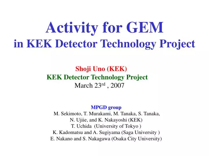
Activity for GEM in KEK Detector Technology Project. Shoji Uno (KEK) KEK Detector Technology Project March 23 rd , 2007. MPGD group M. Sekimoto, T. Murakami, M. Tanaka, S. Tanaka, N. Ujiie, and K. Nakayoshi (KEK) T. Uchida (University of Tokyo )

E N D
Activity for GEMin KEK Detector Technology Project Shoji Uno (KEK) KEK Detector Technology Project March 23rd , 2007 MPGD group M. Sekimoto, T. Murakami, M. Tanaka, S. Tanaka, N. Ujiie, and K. Nakayoshi (KEK) T. Uchida (University of Tokyo ) K. Kadomatsu and A. Sugiyama (Saga University ) E. Nakano and S. Nakagawa (Osaka City University)
Contents • Basic study of GEM • Effective gas gain • Charge distribution • Thicker GEM : 100mmt • Recovering for damaged GEM • Applications • Neutron counter
1mm TestChamber PCB 55Fe (5.9 keV X-ray) DRIFT 10 mm □15mm×15mm GEM1 TRANSFER 1 ~2 mm 36=6×6 GEM2 TRANSFER 2 ~2 mm GEM3 ~2 mm INDUCTION 2200pF PCB 2200pF GAS Ar-CH4(90/10) (P-10) Ar-CO2(70/30)
Signal from GEM foil 150mV Signal from Readout pad 80ns Pulse shape
Readout System For beam test Timing Information CLK Gen.(1MHz) Scaler 1ms Fanin-Fanout Reset T0 timing Trg. Gate Coincidence Gate Gen. CCNET Gate Gen. Gate Gen. 4ms delay Width 40ms GATE GATE CAMAC RPN220 Discr. 120μs delay 5 m BUSY VETO Belle-CDC Pre-amp. RPN220×7 Gated trg. 30 m GATE Belle-CDC Pre-amp. ×7 CAMAC ADC 2249A×9
P10 Ar-CO2 Effective gas gain vs ΔVGEM
Gas gain vs various parameters P10 Ar-CO2 P10 Ar-CO2 EI ED Ar-CO2 P10 Ar-CO2 EI ET
Electric Field Dependence in Drift Region ED=500V/cm ED=3000V/cm EI=1000V/cm EI=1000V/cm 55Fe (5.9 keV X-ray) Drift region ED Normalized Effective Gain ΔVGEM=360V ET=1.6kV/cm EI=3.6kV/cm Electric Field in Drift Region (kV/cm) Low Field in Drift Region High Field in Drift Region Collection efficiency deceases in higher electric field, since some electric field lines reach on the surface of GEM. ΔVGEM=320V ΔVGEM=320V
Electric Field Dependence in Induction Region ED=3000V/cm EI=1000V/cm 55Fe (5.9 keV X-ray) ΔVGEM=350V ED=1.3kV/cm ET=2.1kV/cm Normalized Effective Gain Induction Region EI Electric Field in Induction Region (kV/cm) Low Field in Induction region High Field in Induction Region ED=3000V/cm Extraction efficiency increases in higher electric field, since most of field lines do not go back on the surface of GEM. Additional gas amplification starts for rather high electric field in the induction region. ΔVGEM=320V ΔVGEM=320V EI=4000V/cm
Electric Field Dependence in Transfer Region Ar-CO2 ΔVGEM=350V ED=1.3kV/cm EI=5.95kV/cm Transfer region plays as a extraction of upper GEM and also as a collection of lower GEM. Therefore, the electric field dependence can be represented based on the drift field dependence and the induction field dependence. 55Fe (5.9 keV X-ray) ET Transfer Region ET Transfer Region Eff(ET) Normalized Effective Gain {Eff(ED)×Eff(EI)}2 Electric Field in Transfer Region (kV/cm)
100mm Zoom up view Readout strip 100mm • Readout strip • Strip pitch : 200 mm • width : 100 mm • gap :100 mm • length : 50mm • Number of strips = 64 200mm
OneEventDisplay ADC ADC 63 0 63 0 Channel Channel
Charge distribution ADC SUMADC P10 s = 359.7±0.4 mm ΔVGEM=330V Ed= 0.5 kV/cm Et=1.65 kV/cm Ei= 3.3 kV/cm Ar-CO2(70/30) s = 181.2± 0.3 mm ΔVGEM=370V Ed= 0.5 kV/cm Et=2.59kV/cm Ei=5.18 kV/cm -1 0 1 -1 0 1 dX(each strip-COG) mm Triple GEM gD, gT1, gT2, gI=1.5, 1, 1, 1mm
Measurement results s for a gauss fit in a charge distribution Unit : mm Total gap : gD/2 + (gT1+ gT2 ) + gI
Data MagBoltz P10 s2 (mm2) Ar-CO2
MagBoltzvs.Measurement Data Data MagBoltz P10 Ar-CO2 Electric field in transfer region (kV/cm)
1mm Single GEM-100mm Test Chamber PCB GAS Ar-CO2(70/30) □15mm×15mm 36=6×6 ED=0.75kv/cm EI=7kv/cm 55Fe (5.9 keV X-ray) Drift Plate 2mm Drift Aria→ED 100mm-GEM1 2200pF Read out 2mm Induction Aria →EI PCB Read out 2200pF
Single GEM ΔVGEM Ed=1.5kv/cm Ei=6.0kv/cm
ED dependence90f V.S. 70f ΔVgem=660V Ei=6.0kv/cm
Normal Damaged Recovering • We try to recover the damaged GEM. • Soft etching • Chemical etching • Plasma etching There are damaged spots. Zoom Dead GEM
As a result of recovering • Soft etching • Etching time is shorter than usual chemical etching. • Plasma etching • An etching effect is stronger than chemical etching. • Damaged GEMs, which can not be recovered by soft etching , are reprocessed by Plasma etching. Recovery of GEM is basically possible. • About 90% of Damaged GEMs can be recovered by Soft or Plasma etching .
Detection of Thermal Neutron • No need of expensive 3He Gas • No need of pressure vessel • Free readout pattern • High resolution • Position and Time • Insensitive against g-ray • Capability against high counting rate n Ar-CO2 gas GEM1-B 1 mm a GEM2-B 1 mm 1 mm 2 mm GEM3-Cu 8 foils for real test chamber Readout board
Neutron (2.2Å) 100nsec 200mV/div Signal Shape and Pulse Height Distribution Threshold for g-ray measurement Threshold for Neutron measurement ADC counts
Imaging Data using Radioactive Source 83×83mm2 1.6mm pitch XY strip
Detection Efficiency • 1mmφPin Hole • 3HeCounter • 72413counts/100sec • Boron-GEMFoil • 17355counts/100sec • Detection Efficiency • 24.0% • with 8 GEM foils • Boron-10 : 0.6mmt 1.2mmt per one GEM foil
Position Resolution with 0.5mmf pin hole 2D Log scale 1D Liner scale Strip pitch : 1.6mm
Diffraction Pattern forSingle Crystal K2SeO4 λ= 2.2Å Sample Neutron Beam ~40° ~90° 2q
λ= 2.2Å Single CrystalNaCl 2q = 50°(0,0,2) 2q = 38°(1,1,1) 2q = 76°(0,2,2) 2q = 90°(1,1,3)
Small Angle Scattering at NOP Sample Silica Particle (SiO2) Hypresica HPS 500nm Direct Beam HPS 200nm Background
Summary • In order to understand features of GEM chamber, we have measured effective gas gain and charge distribution for various parameters. • We started to produce new type of GEM to get higher effective gas gain with a single GEM configuration. • Recovering for damaged GEM succeed with large probability. • Neutron counter with Boron coated on the GEM was constructed and tested. Results show it is promising as neutron detectors at neutron facility in J-PARC.
10cm 10cm GEM foils made by Japanese company • New method (plasma etching) was tried in a few years ago. • Not chemical etching (CERN) • M. Inuzuka, et al., NIM A 525(2004) 529-534 • Plasma + Laser • To reduce sparks • It is convenient for us to make new types of GEM foils. • Fine pitch/small hole : 50mm/30mm • Thicker/thinner : 100(150)mm/ 25mm • Other activities in Japan • Tokyo Univ. • RIKEN • etc • Today, I will report on results with standard GEM foils. • 50mm thick • 140mm pitch 70mm diameter Scienergy Co., Ltd. (Japanese company) http://www.scienergy.jp/
Signal Shape and Timing Signal Shape 200nsec T0 Signal within gate Gate 4msec-44msec
3HeCounter Chamber 2q Cd slit Cd slit Sample Diamond Powder Beam Time dependent Diffraction Pattern for Diamond Powder at KENS Time slice without Cd slit
Mono-crystalK2SeO4 Sample Neutron Beam Cd plate Sample 14mm Cd Plates (5mm x 5mm) 1mm Al plate Drift plane GEM1 Same high voltage was supplied on Al plate as that on plate of drift plane.
Mono-crystal K2SeO4 Laue spots Counts/0.1msec 83mm Simlation L=26m 2q=65deg. 83mm by Kamiyama Flight time (Wave length) msec
最後に • 高エネルギー加速器研究機構素粒子原子核研究所 測定器開発室 MPGDグループ • KEKIPNS 宇野彰二(shoji.uno@kek.jp)、 関本美智子、 村上武、 田中真伸、 氏家宣彦、 仲吉一男 • 佐賀大理工 門松宏治、 杉山晃 • 大阪市大理 中川真介、 中野英一 • 東京理科大理工 杉山史憲 • 東京大理 内田智久 • GEM • CERN製 • http://ts-dep-dem.web.cern.ch/ts-dep-dem/products/gem/ • 日本製 サイエナジー株式会社 • http://www.scienergy.jp/ • 海外でのGEM型中性子検出器 • http://www.physi.uni-heidelberg.de/physi/cascade/index.html
Naive estimation using MagBoltzwithout GEM structure 55Fe (5.9 keV X-ray) Electric field : MagBoltz gD ED : σd(E=ED) gT1 ET1 : σd (E=ET1) gT2 ET2 : σd (E=ET2) gI EI : σd(E=EI) σd2=σd(E=ED)2 ×gD/2 + σd(E=ET1)2×gT1+ σd(E=ET2)2×gT2 + σd(E=EI)2×gI
MagBoltz data P10 Ar-CO2
EI dependence90Φ ,V,S 70Φ Ed=1.5kv/cm ΔVgem=660V
Source Test 252Cf (<En>=2.14MeV) Energy (eV) 1MeV 10meV Water Test chamber Moderator
Thickness of Boron-10 Number of counts Thickness of B-10 per GEM foil (mm)
Detection efficiency vs Number of Foils Thickness of B-10 : 1.2mm/foil(single side:0.6mm) Number of counts Number of B-10 GEM foils
2D Readout Board Y(Rear) X,Y Strip Strip pitch1.6mm Number of strips52×52 Active area83mm×83mm X
27 mm =17 x 1.6mm 83mm 27 mm Slit Slit 83mm Image data with Neutron Beam Beam Profile Cd slit with ”K”