Download
1 / 77
770 likes | 815 Views
Learn about signal flow graphs & microstrip line design in microwave techniques. Understand matching transformers & practical fabrication methods. Step-by-step guide to using VNA & calibration techniques.

E N D
Lecture 4 • Example of Signal Flow Graphs • Microstrip Line Design and Matching • Multisection Transformer • Binomial Multisection Matching Transformers • Chebyshev Multisection Matching Transformers Microwave Techniques
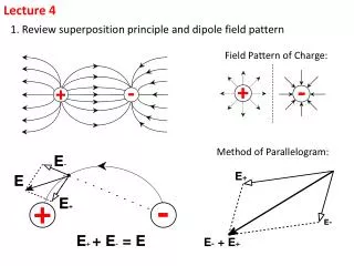
Example of Signal Flow Graphs • use signal flow graphs to find the power ratios for the mismatched three-port network shown below (Problem 5.32, Pozar) Microwave Techniques
Example of Signal Flow Graphs • the signal flow graph is as follows: Microwave Techniques
Example of Signal Flow Graphs • Alternatively, we have Microwave Techniques
Example of Signal Flow Graphs • to relate b2 and a1, we have the signal flow graph is as follows: Microwave Techniques
Example of Signal Flow Graphs • To relate b3 and b2, Microwave Techniques
Example of Signal Flow Graphs • the power ratio must be Microwave Techniques
Example of Signal Flow Graphs Microwave Techniques
Microstrip Line Design and Matching • to design and fabricate a 50 W microstrip line • to design and fabricate a quarter-wave transformer and open-stub matching circuits for matching a 25 W load to a 50 W transmission line at 4 GHz • to use design curves (or computer code) for circuit design and simulations Microwave Techniques
Design of a Microstrip Line • using the closed-form formulas discussed earlier, calculate the width of a 50 W microstrip line • the printed-circuit board has a dielectric constant of 2.6 and thickness of 1.59 mm • assuming the conductor thickness is small, obtain the effective dielectric constant Microwave Techniques
Design of a Microstrip Line • from design curves, we found that W=4.3980 and ee= 2.1462 • fabricate a microstrip transmission line using a conducting tape • the width should be close to the size W • press the conducting tape to eliminate any air gap between the substrate and the conductor Microwave Techniques
Design of a Microstrip Line • for more accurate fabrication, one can use etching techniques • attach one SMA connector as shown below: Microwave Techniques
Design of a Microstrip Line • do a one-port calibration of the vector network analyzer (VNWA) from 0.5 to 10GHz at the end of the flexible cable, assume a fixed load (50W) is a broadband load in the one-port calibration Microwave Techniques
Design of a Microstrip Line • APC-7 is a sexless precision connector which can be used up to 20 GHz • to obtain an accurate amplitude and phase of DUT(device under test), the VNWA must be calibrated at a reference point • the most commonly used OSL method utilizes three standards, Open, Short and Load (50W) Microwave Techniques
Design of a Microstrip Line • the front panel of VNWA has two ports which are designated as Port 1 and Port 2 • some devices have only one port and they are called the one-port devices • TV has only one input, if we want to measure the input impedance of a TV antenna, connect it to either Port 1 or Port 2 and measure the reflection from the antenna Microwave Techniques
Design of a Microstrip Line • because it is common to use Port 1 for the one-port device measurement, we will discuss the S11 (Port 1) calibration • first we need to choose the point at which the calibration is performed • for example, if we want to perform S11 calibration at the end of a long cable, calibration standards Open, Short and Load must be connected at this point Microwave Techniques
Design of a Microstrip Line • after the correct S11 one-port calibration, Short connected at the calibration point should show the reflection coefficient of -1 (0dB and 180o phase) • the calibration point also corresponds to zero second in the time domain Microwave Techniques
Design of a Microstrip Line • note that the APC-7 and the SMA connectors are of different size and therefore, we need an APC-7-SMA adapter Microwave Techniques
Design of a Microstrip Line • as a result, we need to shift the reference plane to the end of the adapter • two options, i.e., port extension and electrical delay can be used • port extension requires the time delay from the original plane to the new calibration plane while electrical delay requires the round-trip time Microwave Techniques
Design of a Microstrip Line • after one-port S11 calibration has been done, attach a short to the end of the microstrip line, obtain the electrical delay to the short from the reference position Microwave Techniques
Design of a Microstrip Line • the short can be achieved by using conducting tape Microwave Techniques
Design of a Microstrip Line • remove the short and attach a SMA connector Microwave Techniques
Design of a Microstrip Line • connect the 25 W load to the SMA connector • measure the input impedance at the load, note that due to imperfect connections, the measured load may have a small imaginary part • we can use a Smith Chart to find out the location on the microstrip line where the input impedance becomes 25 W, here let us assume it is exactly 25 W Microwave Techniques
Design of a Microstrip Line • make a quarter-wave transformer using a conducting tape • quarter-wave transformer can be explained by the following equation Microwave Techniques
Design of a Microstrip Line • there will be no reflection is • Therefore, • and Microwave Techniques
Design of a Microstrip Line • because of the presence of the SMA connector at the end of the microstrip line, it is not convenient to put the quarter-wave transformer there; we can move the 25 W point to l/2 from the load toward the APC-7-SMA adapter Microwave Techniques
Design of a Microstrip Line • the effective dielectric constant is 2.1462, therefore, Microwave Techniques
Design of a Microstrip Line • the length of the quarter-wave transformer is le/4, however, le is different from the one for the 50 W line • the characteristic impedance of the transformer is 35.25 W and from the previous equations, we found W=7.2261 and ee= 2.2193 Microwave Techniques
Design of a Microstrip Line • the length of the quarter-wave transformer is Microwave Techniques
Design of a Microstrip Line • the microstrip line and the quarter-wave transformer are depicted below: • assuming that the total length of the transmission line is 100 mm Microwave Techniques
Design of a Microstrip Line • the magnitude of S11 measured at the left SMA connector looks like: Microwave Techniques
Design of a Microstrip Line • note that this result may be different from measurement, one of the reasons is that we assume the characteristic impedance and effective dielectric constant are independent of frequency • we can make a rough estimation of the bandwidth of this quarter-wave transformer Microwave Techniques
Design of a Microstrip Line • at the designed frequency fo , the reflection coefficient is Microwave Techniques
Design of a Microstrip Line • Assuming a TEM line Microwave Techniques
Design of a Microstrip Line Microwave Techniques
Design of a Microstrip Line • nearby the design frequency, and therefore Microwave Techniques
Design of a Microstrip Line • this function is symmetric about the design frequency, we can define a bandwidth for a maximum value of the reflection coefficient that can be tolerated Microwave Techniques
Design of a Microstrip Line • , the lower value is while the upper value is Microwave Techniques
Design of a Microstrip Line • For a TEM line, • the fractional bandwidth is given by Microwave Techniques
Design of a Microstrip Line • make an open stub using a conducting tape • to derive the formulas for location d and length l of the stub, consider the following equations with t=tan(bd): Microwave Techniques
Design of a Microstrip Line • to match the line, we need G = Yo = 1/Zo Microwave Techniques
Design of a Microstrip Line • solving for t gives Microwave Techniques
Design of a Microstrip Line • the two principal solutions for d are Microwave Techniques
Design of a Microstrip Line • here XL = 0, • d = 51.2(35.26/360)=5.0148mm • this is too close to the SMA connector, we add le/2 = 25.6+5.0148=30.06 mm • the stub susceptance Bs must be negative of B to cancel the imaginary part of the admittance Microwave Techniques
Design of a Microstrip Line • From the equation, • For an open stub • For a short circuit stub, Microwave Techniques
Design of a Microstrip Line • if the length given by these equations is negative, l/2 can be added to give a positive result Microwave Techniques
Design of a Microstrip Line • attach an open-stub matching circuit to the transmission line and obtain the S11 response Microwave Techniques
Design of a Microstrip Line Microwave Techniques
Design of a Microstrip Line • this result may be slightly different from measurement, the open stub has some end capacitance that is being ignored in addition to the frequency dependence of the characteristic impedance and effective dielectric constant Microwave Techniques
Multisection Transformer • consider the reflection from a segment of a transmission line discontinuity depicted below Microwave Techniques