Download
1 / 7
70 likes | 192 Views
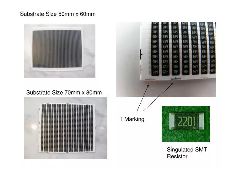
Substrate Size 50mm x 60mm. Substrate Size 70mm x 80mm. T Marking. Singulated SMT Resistor. MK. R T 字線. G1 T 字線. G2 T 字線. C1 T 字線. G2 T 字線. G1 T 字線. R T 字線. MK. R T 字線. R T 字線. G1 T 字線. G1 T 字線. G2 T 字線. G2 T 字線. 49.5mm. C1 T 字線. C1 T 字線. G2 T 字線.

E N D
Substrate Size 50mm x 60mm Substrate Size 70mm x 80mm T Marking Singulated SMT Resistor
MK R T字線 G1 T字線 G2 T字線 C1 T字線 G2 T字線 G1 T字線 R T字線 MK R T字線 R T字線 G1 T字線 G1 T字線 G2 T字線 G2 T字線 49.5mm C1 T字線 C1 T字線 G2 T字線 G2 T字線 G1 T字線 G1 T字線 R T字線 R T字線 R T字線 G1 T字線 G2 T字線 C1 T字線 G2 T字線 G1 T字線 R T字線 MK MK 60mm T marking on substrate
<12mm <12mm R T字線 G1 T字線 G2 T字線 G1 T字線 R T字線 C1 T字線 <9mm C1 T字線 <9mm R T字線 R T字線 G1 T字線 G1 T字線 MK MK 49.5mm G2 T字線 G2 T字線 MK MK G1 T字線 G1 T字線 R T字線 R T字線 <9mm <9mm C1 T字線 R T字線 G1 T字線 G2 T字線 G1 T字線 R T字線 C1 T字線 <12mm <12mm 60mm
Process of making the SMT resistor 1st silk screen printing is C1 (Silver color) This is the silver conductive pad on both side of the resistor 2nd Silk screen printing is R (Black color) This is the carbon film that control the resistor value Next is G1 (Light Green colour) This is a protective cover for carbon resistor Next is Laser Trimming L cut using LaserTek machine Last is Silk Screen printing is G2 (black color) Protective cover after trimming
As each layer is being printed, T marking is printed as marking Vision have to inspect the T marking to check that each layer is over lapping correctly. The T marking is also use to check if the printing is at the correct position on the ceramic substrate by using the ceramic edges as reference. The other inspection is to look for defect. If defect is found the unit need to be marked out by laser cut across the unit.
Current demo machine is their production line is using a 12M pixel camera. I suspect they are using a color camera as the manager is not able to confirm The inspection time and cutting for 2% fail parts per 5540 resistor per substrate is between 4.5 to 5sec.
12 Mega Pix Colour Camera Yag Laser Lens FOV for 70x80mm Substrate Laser Scan Head with 100mm x 100mm FOV Blue LED lighting Ceramic Substrate Back LIght Ceramic Substrate Substrate Input Elevator Substrate Output Elevator Substrate NG Output Elevator Actuator Substrate Work Holder