Download
1 / 27
290 likes | 693 Views
Presentation on SGS, Crystal Defects & Wafer Preparation. Guided By MD. Mohiuddin Munna. #Group Members#. Chinmoy Das (2010338012) Nazmul Hossain (2010338016) Niloy Bonik (2010338017) Sohel Rana (2010338033). #Semiconductor Grade Silicon (SGS)#.

E N D
Presentation on SGS, Crystal Defects & Wafer Preparation Guided By MD. Mohiuddin Munna
#Group Members# • Chinmoy Das (2010338012) • Nazmul Hossain (2010338016) • Niloy Bonik (2010338017) • Sohel Rana (2010338033)
#Semiconductor Grade Silicon (SGS)# • The highly refined silicon used for wafer fabrication. • Also known as Electronic Grade Silicon. • Has ultra high purity.
#Steps to obtaining SGS# • Obtaining MGS
#Steps to obtaining SGS# • Pure Silicon Producing System
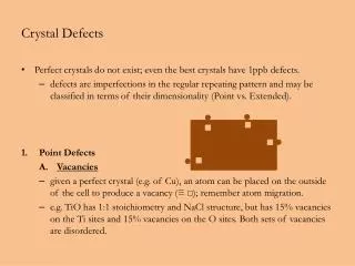
#Crystal Defects in Silicon# • Interruption in the repetitive nature of the unit cell crystal structure. • Aiso known as micro defect.
#Types of Defects# • Point Defects: Localized crystal defect at the atomic level. • Dislocations: Displaced unit cells. • Gross Defects: Defects in crystal structure.
#Point Defects# • Vacancy Defect • Interstitial Defect • Frenkel Defect
#Wafer Preparation# • A process of preparing wafer including- • Machining operations • Chemical operations • Surface polishing & • Quality measures.
#Steps’ Introduction# • Crystal Growth • Shaping • Wafer Slicing • Wafer lapping & edge grind • Etching • Polishing • Cleaning • Inspection • Packaging
#Shaping Operations# End Removal Diameter Grinding
#Wafer Lapping# • Two-sided lapping operation to remove damage left by slicing. • Performed under rotational pressure with pads & mixture of alumina or silicon carbide & glycerin.
#Cleaning# • Wafers must be cleaned to achieve an ultraclean state. • Wafers should be free of particles & contamination.
#Wafer Evaluation# • Wafers need to be inspected carefully before packaging. • Standard quality should be measured.
#Packaging# • Finally wafers should be packaged carefully.
Here is the END of our presentation Thanks everyone for being with us