Download
1 / 41
480 likes | 1.05k Views
The design of the TimePix chip. Xavier Llopart, CERN MPI-Munich, October 2006. 50um. Micromegas. GEM. From Medipix to Timepix. A novel approach for the readout of a TPC at the future linear collider is to use a CMOS pixel detector combined with some kind of gas gain grid

E N D
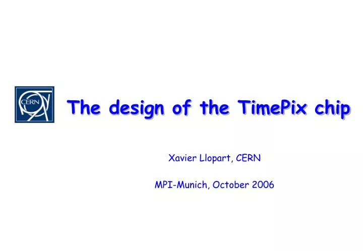
The design of the TimePix chip Xavier Llopart, CERN MPI-Munich, October 2006
50um Micromegas GEM From Medipix to Timepix • A novel approach for the readout of a TPC at the future linear collider is to use a CMOS pixel detector combined with some kind of gas gain grid • Using a naked photon counting chip Medipix2 coupled to GEMs or Micromegas demonstrated the feasibility of such approach
Motivation • These experiments (by NIKHEF/Saclay, Freiburg 2004/2005 ) demonstrated that single electrons could be detected using a naked Medipix2 chip 2D • Did not provide information on the arrival time of the electron in the sensitive gas volume 3D (position + time) !!! • To further exploit this approach the Medipix2 is being redesigned to incorporate a time stamp with a tunable resolution of 100 to 10ns. • Requirements: • Keep Timepix as similar as possible to Medipix2 in order to benefit from large prior effort in R/O hardware and software • Avoid major changes in pixel and/or readout logic – risk of chip failure due to poor mixed mode modelling • Eliminate 2nd threshold • Add possibility of programming pixel by pixel arrival time or TOT information • This modification is supported by the JRA2/EUDET Collaboration (www.eudet.org)
Medipix → Timepix: Analog side changes • Changes in Preamp: • Added cascode to preamp • Changes in the discriminator: • Only 1 discriminator • 4-bit threshold equalization • Polarity control • Added hysteresis
Medipix → Timepix: Preamplifier change • Added cascode (8-bit DAC controlled): • Gain ↑ (~18mV/Ke-) keeping Voutrms noise cte → SNR ↑ • Expected ENC 75e- • Expected Linearity: 0.6 to 1.5 Volts → 50Ke- linear range • Expected Missmatch: vt 2.11mV → vt 117e-
Medipix → Timepix: Preamp Out vs Ikrum DAC • 18.75 Ke input charge • Ikrum DAC set: 5, 10, 20 and 40 • Direct measurement on the Timepix test output pads 50mV 1 μs • 18.75 Ke input charge • Ikrum current set: 1.7, 3.4, 6.8, 13.6 nA
Medipix → Timepix: Gain Linearity • Expected gain linearity up to ~50Ke- • >50Ke- the Preamp output saturates 50mV 1 μs 50mV 1 μs Simulation Measurement: ∆Qin and ∆Ikrum
Medipix → Timepix: Preamp Out vs Preamp DAC • Gain (ENC noise) depends on the preamp current • Tunable peaking time: ~90ns to 400ns → check Time-walk! 50mV 200 ns Lower Preamp current
TestPulse on 1 pixel (Medipix Mode) Ikrum=5 Gain is ~16.06mV/Ke- (Ikrum=5) σ ~ 3.9 DACs ~98e- rms Pixel Min Threshold < 500e-
Medipix → Timepix: Discriminator changes • Added hysteresis (8-bit DAC controlled) in discriminator: • ~200e- lower threshold and no glitches at the disc output • It can be turned off • Polarity selection on the discriminator: • Hysteresis possible • Optimization of the zero crossing design • 4-bit threshold adjustment: • Expected Threshold dispersion after adjustment ~25e-
Medipix → Timepix: Time walk Simulation-Measurement • Measured timewalk with the default DAC values • Possible offline correction combined with TOT measurement can bring timewalk < Ref_Clk period Simulation Measurement: ∆Thr
Medipix → Timepix: TOT vs Ikrum (simulation) Ikrum=5nA (~55nA/Ke-) Ikrum=10nA (~28nA/Ke-) Ikrum=20nA (~14nA/Ke-) • TOT Linearity > 200 Ke-
Medipix → Timepix: TOT vs Ikrum (measurement) • TOT gain is a function of Ikrum DAC setting • Ref_Clk=71.1MHz
Timepix equalization (I) • Equalization using the noise as trigger and Medipix Mode (P0=P1=0) • The measured DNL of the 4-bit DAC is < 1THL DAC -> Interpolation in the equalization can be used µ=7591.8 σ=1.48 (~36.8 e-) µ15=7561.5 σ15=9.01 (225 e-) µ0=7624 σ0=9.13 (228 e-)
Analog pixel summary • Maximum possible Qin injected via Testpulse is ~50Ke-
Medipix → Timepix: Digital side changes • Added time reference (Ref_Clk) • Selectable operation modes (P0 and P1) • TSL (Timepix synchronization Logic) • Pixel-by-pixel synchronized Shutter
Medipix → Timepix: Added Time reference (I) • Column length= 55x256= 14080μm • W=0.4μm,T=0.54μm, H=0.8μm • R2.8KΩ • Ctot<=2pF • Parasitic cap negligible at D>3 μm Ctot Cline-GND + Cline-VDD Cline-Cline
Medipix → Timepix: Added Time reference (II) N buffer per column: • Min size buffer inverter per pixel • No differential signals needed • Power uniformly distributed over clock period • N=256, f=100MHz • Propagation delay = ~50ns (~195ps/inv) • Simulation takes care of parasitic capacitances and top-down resistive power lines. ~50ns ~0.820mA/col ~210mA/chip
Medipix → Timepix: Expected digital power dissipation • Pvdd=V2·f·Ctot • Simulation @ Vdd=2.2V but digital part could work to 1.8V (33% less power) Ivdd[mA] 2·f[MHz]
Medipix → Timepix: TSL • Use of 3-bit High threshold adjustment bits for : 4th equalization bit and P0, P1. • Each pixel can be configured independently in 5 different modes. • This logic needs 128 Trts (Mpix2MXR20 had 92 Trts)
Core Timepix Synchronization Logic (TSL) • Hit is synchronized with Ref_Clk and Shutter generating the signal to the counter and internal Shutter depending on P0, P1 and Mask bits. • Power consumption only when Hit is present • TSL Core is divided in 2 blocks: Core1 used for the Timepix and TOT modes and Core2 used for Medipix mode. • Core blocks have being designed using an asynchronous network with S-R Flip-flops with race-free state assignment
2 2 2 1 7 4 5 4 5 1 8 8 1 5 4 5 7 1 3 4 3 1 4 6 4 8 TSL Core1 Asynchronous design • TSL desired time diagrams 7,4 1,2,3 Hit (X1) Clock (X2) Z1=0 Z2=0 Z1=1 Z2=0 4 5,4 8 1 Gate Clock (Z1) 1 Z1=1 Z2=1 Z1=1 Z2=1 To Counter (Z2) 5 1 5,6 8 • State diagram
TSL Core Asynchronous design (II) 01 7,4 00 1,2,3 Z1=0 Z2=0 Z1=1 Z2=0 Z1=0 Z2=0 Z1=1 Z2=0 4 4 5,4 8,5* 8 1 1,4* 1 Z1=1 Z2=1 Z1=1 Z2=1 Z1=1 Z2=1 Z1=1 Z2=1 5,1* 5 10 11 5,6 8 • State diagram • Reduced State diagram
TSL Core Asynchronous design (III) Conf 01 00 Z1=0 Z2=0 Z1=1 Z2=0 4 8,5* 1,4* Z1=1 Z2=1 Z1=1 Z2=1 5,1* 10 11 • Implementation with SR flip-flops (62 trts) • Reduced State diagram with initialization
3 5 4 5 4 1 2 5 4 3 2 1 3 1 1 2 TSL Core2 Asynchronous design Gate Clock (Z1) To Counter (Z2) Medipix2 (Z3) • Implementation using gates (20 trts) since inputs are race-free “by design” • TSL desired time diagrams
Timepix Mode (P0=1,P1=1) 17 164 10MHz 100MHz
TOT Mode (P0=1,P1=0) 33 50 12 2Ke- 4Ke- 2Ke- 10MHz 100MHz
Medipix Mode (P0=0,P1=0) 10MHz 100MHz
Internal Shutter control • Internal Shutter is always synchronous to the clock to avoid glitches • Counter starts counting if a hit is present when shutter starts • Shutter closing happens with a maximum delay of 1Tclk if a hit is present when shutter closes
Digital power consumption • Reduce digital power of the TSL cores → No power consumption in stand-by (no hit) • In stand-by the only digital consumption is the buffering of the Ref_Clk • Controlled by design of the core1 asynchronous network.
Shutter PreampOut Thr discOut CounterClk Pixel measurements • From the 2 test pixels [120:121,0] one can measure the preampOut, discOut, internal Ref_Clk and the counter clock • State Machine of the counter Modes (P0, P1) work as expected • No visible coupling of the Ref_Clk signal into the analog signals (preampOut and discOut)
Timepix Layout status Mpix2MXR20 layout Timepix layout
Timepix chip architecture • Chip architecture almost identical to Mpix2MXR20 • M0=M1=1 and Shutter ON -> FClock used as Ref_Clk • 256x256 55µm square pixels • Analog Power -> 440mW • Digital Power (Ref_Clk=50MHz) -> 220mW • Serial readout (@100MHz) -> 9.17 ms • Parallel readout (@100MHz) -> 287 µs • > 36M Transistors
Periphery Verilog Simulations • This simulation tests 1 row of pixels and the full chip control logic • Tested with normal and corner (3) parameters successfully • Pixel control logic is initialized after a set mask command • M0=1 and M1=1 when counting will enable the clock distribution to the pixel matrix
Single chip Verilog simulation 1:SetDACs 2:SetMatrix 3:ResetMatrix (PS=1) 4:Counting 5:Readout (PS=1) 1 2 3 4 5
Counting Modes (Mask,P0 and P1) Pixel Masked P0=X, P1=X and Mask=1 Tpix-1h mode P0=0, P1=1 and Mask=0 Mpix2 mode P0=0, P1=0 and Mask=0 Tpix mode P0=1, P1=1 and Mask=0 CCD mode P0=1, P1=0 and Mask=0
Summary & Conclusions • Timepix is a modification of the Medipix chip • Improvements in Gain and threshold equalization -> expected lower threshold (~900e- → ~600e-) • Pixel operation mode is selectable for each pixel • TimeStamp reference (Ref_Clk) generated by a common clock distributed all over the chip • Timepix time line: • Desgin: 6 months (January06-June06) • Fabrication: 2 months (July06-August06) • Testing: 1 months so far ( mid September06-?)