Download
1 / 20
330 likes | 895 Views
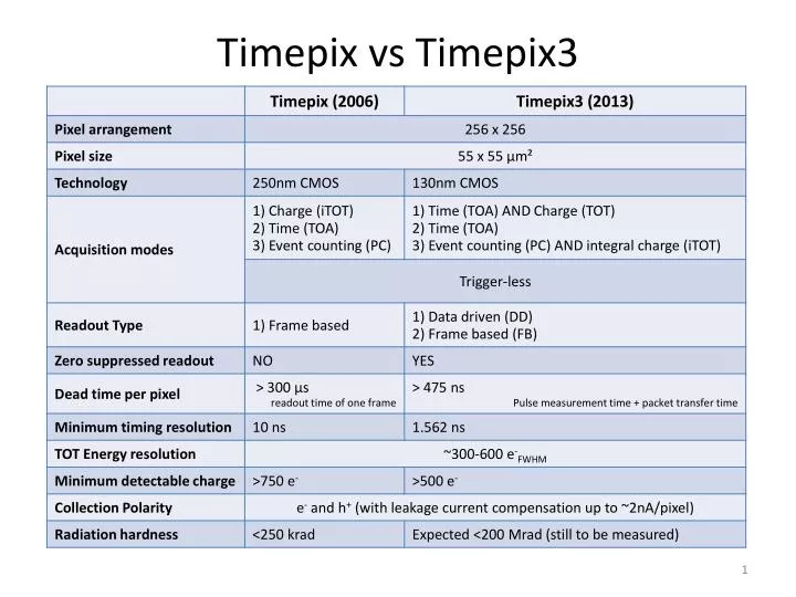
Timepix vs Timepix3. Timepix (2006). Broad experience with different type of sensors: Si N-on-P, P-on-N (from 50um to 2mm thick) and edgeless CdTe w ith Ohmic and Schottky contacts (1mm) GaAs (500um) >350 paper citations >200 wafers produced (107 chips/wafer)

E N D
Timepix (2006) • Broad experience with different type of sensors: • Si N-on-P, P-on-N (from 50um to 2mm thick) and edgeless • CdTewith Ohmic and Schottky contacts (1mm) • GaAs (500um) • >350 paper citations • >200 wafers produced (107 chips/wafer) • Access to Timepix wafers possible • Different readout systems available from the Medipix2 collaboration: • Most versatile DAQ is FITPIX. USB interface from CTU Prague (http://www.widepix.cz)
Timepix3 (2013) • Chip available since September 2013: • Chip is fully functional • Currently running the first wafer probing campaing prior bump-bonding to standard Si sensor (300 µm) • Difficult availability to chips/wafers: • Priority to cover the Medipix3 collaboration needs • 12 wafers available (105 chips/wafer) • Production run (48 wafers) to be ordered as soon as first Si assemblies validate the chip performance • 3 readout DAQ under design: • SPIDR (NIKHEF/CERN) 10 Gbps link • FITPIX3 (Prague) USB 2.0 link • MERLIN (Diamond, UK)
Frame basedand zero-supressed readout • Maximum frame rate: 1300 fps @5.12Gbps Acquisition time Shutter Qin DataOut 48bit 48bit 48bit 48bit 48bit 0x71 0xA0 ChipID [32b] Address[16-bit] Data[28-bits] 0xA End of Command (48 bits) Data Packet (48 bits)
Event-by-event data driven and zero-supressed readout • Achievable count rate: • uniformly distributed events →~40 Mhits/s/cm2 @5.12Gbps • Full matrix readout: ~800 µs @5.12Gbps Acquisition time Shutter Qin DataOut 48bit 48bit 48bit 48bit 48bit 48bit 0x71 0xB0 ChipID [32b] Address[16-bit] Data[28-bits] 0xB Data Packet (48 bits) End of Command (48 bits)
Pixel Operation in TOA & TOT Tpeak< 25ns Preamp Out Disc Out Pixel Readout Starts (475ns→ 19 clock cycles) Clk (40MHz) Global TOA (14-bit) 16382 16383 16384 0 1 2 3 4 VCO Clk (640MHz) FTOA (4 bits)=7 TOA (14-bit) X 16383 TOA (14 bits)=16383 TOT Clk (40MHz) TOT (10 bits) =4
Pixel Operation in TOA only Tpeak< 25ns Preamp Out Disc Out Pixel Readout Starts (475ns→ 19 clock cycles) Clk (40MHz) Global TOA (14-bit) 16382 16383 16384 0 1 2 3 4 VCO Clk (640MHz) FTOA (4 bits)=7 TOA (14-bit) X 16383 TOA (14 bits)=16383
Pixel Operation in PC and iTOT Preamp Out Disc Out Pixel readout can start in Data Driven or Frame based Clk (40MHz) Shutter 0 1 2 3 4 5 iTOT (14-bit) iTOT (14 bits)=5 0 1 2 3 PC (10-bit) PC (14 bits)=3
Timepix3 Pixel Schematic TOA (14-bit) TOT (10-bit) FTOA (4-bit) TOA (14-bit) FTOA (4-bit) iTOT (14-bit) PC (10-bit) 1 pixel Common for 8 pixels Front-end (Analog) Front-end (Digital) Super pixel (Digital) Leakage Current compensation Token arbitration TOA & TOT Deserializer [1x31] TOA 3fF Input pad PC & iTOT 31-bits Preamp Counters & Latches Synchronizer & Clock gating Super pixel FIFO [2x31] TestBit MaskBit ~50mV/ke- 14-bits VCO @640MHz 4-bit Local Threshold 3fF 640MHz 37-bits handshake TpA TpB Global threshold (LSB= ~10e-) clock (40MHz) Time stamp OP Mode Data out to EOC Control voltage clock (40MHz)
14080 µm Timepix3 Active Periphery 64 VCO control voltage buffers VCO Buffer [0] VCO Buffer[2] VCO Buffer[63] Buffered bias voltages EoC[2] EoC[0] EoC[1] EoC[126] EoC[127] 128 End of Column logic VCO bias 640MHz Bus Controller 1260 µm Analog Periphery Control Logic Periphery bus (3.84Gbps) Slow Control & Command Decoder PLL 8x Serializer 8b10b DDR 1 BandGap 18 Global DACs E-Fuses 32 bits Clk40 Data output DDR 8b10b encoding (1 to 8 links) Up to 8x640 Mbps (5.12 Gbps)
14100 µm Timepix3 Layout • Analog Front-End: • 13x55 μm2 • <25% pixel area • Double column: • 2x256pixels • 64 super pixels • IO Pad on digital area: • Careful shielding • Pad is ½ of Timepix 55 µm • VCO (FTOA): • 9.6x20 μm2 • < 0.8% SP area 55 µm Sensitive Area (14080 µm) • Full Pixel Matrix: • 256x256 pixels • 128 double columns • 8192 VCOs (640MHz) • 177 Mtransistors 16210 µm • Super Pixel (SP): • 2x4 pixels • 110x220 μm2 Active Periphery Active Periphery (1260 µm) Pad Extenders: Removed if TSV Pad extenders (870 µm)
Medipix chip family Clicpix (2013) Timepix3 (2013) Timepix (2006) Medipix3RX (2011) Medipix2 (1998) Medipix1 (1998)
Timepix3 readout → SPIDR (Nikhef) • Speedy PIxelDetector Readout (SPIDR): • Readout system for Medipix3 and Timepix3 (single upto quads) • 1 x 10Gbps Ethernet link IO • First chips available since beginning of September • All measurements reported use data readout @640Mbps/link Timepix3 Chip 10 Gbit Ethernet Virtex 7 FPGA VC707 Evaluation Board ESE Seminar – X.Llopart
Timepix3 CERN PCBs Timepix3 CERN chip board Timepix3 Probe card Timepix3 translator FMC/VHDCI ESE Seminar – X.Llopart
250 Test Pulses in 1 pixel [Threshold scan in PC & iTOTmode, 1 pixel] ENC ~5.7 LSBrms = ~60 e- Assuming: Ctest=3fF → Tpulse=20e-/mV ESE Seminar – X.Llopart
Full Matrix ENC[Threshold scan over noise floor in PC & iTOT mode] µ = 59.9e- σ= 2.85e- 15 pixels ENC > 80e- 9 pixels not responding • ENC matches predictions from simulations • No significant digital coupling into analog FE ESE Seminar – X.Llopart
Pixel-to-pixel Threshold Equalization[Threshold scan over noise floor in PC & iTOT mode] µeq = 0e- σeq= 35e- µF = 762e- σF= 197e- µ0 = -762e- σ0= 195e- Pixel DAC = 0x0 Pixel DAC = 0xF ESE Seminar – X.Llopart
Full chip minimum threshold [Equalized pixel matrix, 16 pixels masked] ~100e- TOA and TOT (VCO ON) ~500e- ENC of ~77e-rms PC and iTOT ~400e- ENC of ~60e-rms ESE Seminar – X.Llopart
More information • Timepix3 PH-ESE seminar to come Feb. 25:http://indico.cern.ch/event/267425/ Everybody welcome to join.