Download
1 / 18
180 likes | 333 Views
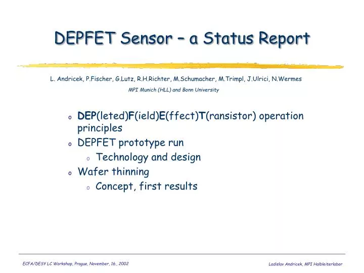
DEPFET Sensor – a Status Report. L. Andricek, P.Fischer, G.Lutz, R.H.Richter, M.Schumacher, M.Trimpl, J.Ulrici, N.Wermes. DEP (leted) F (ield) E (ffect) T (ransistor) operation principles DEPFET prototype run Technology and design Wafer thinning Concept, first results.

E N D
DEPFET Sensor – a Status Report L. Andricek, P.Fischer, G.Lutz, R.H.Richter, M.Schumacher, M.Trimpl, J.Ulrici, N.Wermes • DEP(leted)F(ield)E(ffect)T(ransistor) operation principles • DEPFET prototype run • Technology and design • Wafer thinning • Concept, first results MPI Munich (HLL) and Bonn University Ladislav Andricek, MPI Halbleiterlabor
radiation 55Fe-spectrum @ 300K single pixel ~1mm - - - + - + - + + - ENC = 4.8 +/- 0.1 e- DEPFET Sensor - Principle of operation (e.g.JFET) - ~300 mm Advantages: Amplification of the charge at the position of collection => no transfer loss Full bulk sensitivity Non structured thin entrance window (backside) Very low input capacitance => very low noise Ladislav Andricek, MPI Halbleiterlabor
DEPFET Sensor - linear MOSFET for small pixel - MOS transistor instead of JFET A pixel size of ca. 20 x 20 µm² is achievable using 3µm minimum feature size. Ladislav Andricek, MPI Halbleiterlabor
switch on row & common source readout clear internal gate DEPFET Matrix - Principle of operation - Ladislav Andricek, MPI Halbleiterlabor
Pre-test diodes IBulk =100pA/cm2 -> like in old technology DEPFET Sensor- Technology Development - Self aligned double poly / double aluminium process on high ohmic n- substrate along p-channel Ladislav Andricek, MPI Halbleiterlabor
DEPFET Sensor- Layout - • 2 pixels • 30 x 30 µm² • DEPFET • L = 5 µm • W = 18 µm • reduce the required read out speed by 2 doubles the number of read out channels Ladislav Andricek, MPI Halbleiterlabor
N-side view with two polysilicon layers and contact openings 1 Pixel cell Drain Gate Still to do: - P-side processing - Metallization Clear Expected to be finished: Spring 2003 Clear gate Source DEPFET Sensor- prototyping/current production status - Many test arrays on a 6“ Wafer - Circular and linear DEPFETS up to 128 x 128 pixels minimum pixel size about 30 x 30 µm² - variety of special test structures Ladislav Andricek, MPI Halbleiterlabor
Processing thin detectors- the Idea - Ladislav Andricek, MPI Halbleiterlabor
Processing thin detectors- Wafer bonding - 10 “SOI” Wafer prepared by MPI für Microstrukturphysik, Halle ≈1 cm/sec picture from: www.mpi-halle.mpg.de Q.-Y. Tong and U. Gösele “ Semiconductor Wafer Bonding ” John Wiley & Sons, Inc. Ladislav Andricek, MPI Halbleiterlabor
Processing thin detectors- anisotropic wet etching - Hydroxide etching of silicon: KOH, NaOH, … , TMAH: (CH3)4 NOH Ladislav Andricek, MPI Halbleiterlabor
Processing thin detectors- first tests - Handle Wafer: n-type, 1-100 Ohm.cm, (100), thickness 283 - 297 micron Top Wafer: n-type, 1-3 kOhm.cm, (100) * BOX layer: Oxide 245 nm * wafer bonding * annealing for 4 hours at 1050 ºC to 900 ºC. * grinding and polishing of device wafer (Sico) After bonding, thinning, and polishing top layer thickness: 24 - 29 micron (3 Wafer) 36 - 38 micron (3 Wafer) 43 - 47 micron (4 Wafer) Ladislav Andricek, MPI Halbleiterlabor
Processing thin detectors - first test mask / KOH etching at CiS - Processing at CiS (5 wafer): *deposition of 60nm Si3N4 masking layer on SiO2 *Dry etching of the windows, open oxide layer *KOH etching at 80 ºC *remove nitride layer 50x13 mm2 (tesla/2, one supporting bar) (50x13)/2 mm2 (3 supporting bars) 80x10.4 mm2 (80% of tesla sensor) 6.5x6.5 mm2 (50x13)/4 mm2 (7 supporting bars) drawbacks of KOH etching: 1.) poor selectivity to oxide -> nitride mask 2.) poor selectivity to Al 3.) alkali ions –> not CMOS compatible Ladislav Andricek, MPI Halbleiterlabor
26 μm 51 μm Processing thin detectors - distortions - Ladislav Andricek, MPI Halbleiterlabor
good selectivity to oxide almost perfect selectivity to Al no alkali ions poorer selectivity to (111) (≈30:1) rough surface after etching (hillocks) Etch solution: 5 wt.% TMAH 1.6 wt.% dissolved silicon 0.4 wt.% (NH4)2S2O8 -> at 80 ºC forms a passivation layer on Aluminium pads: Aluminium-oxide Aluminium silcates { } Processing thin detectors - first test mask / TMAH etching at HLL - Tetra-Methyl-Ammonium-Hydroxide Ladislav Andricek, MPI Halbleiterlabor
ATLAS Pixel Detector (Al on 500 nm SiO2) after 10 h at 80 ºC on ≈40 μm thick Silicon Processing thin detectors - TMAH etching at HLL/ results - etch rate (100): ≈35 μm/h etch rate of Al, wet SiO2: < 1 nm!! Ladislav Andricek, MPI Halbleiterlabor
unstructured n+ on top structured p+ in bond region Device Wafer Handle Wafer structured p+ on top unstructured n+ in bond region Processing thin detectors - next steps / status - Diodes on thin silicon: * test bondability of implanted oxide *electrical performance of diodes on thin silicon * process evaluation and more mechanical test Ladislav Andricek, MPI Halbleiterlabor
Processing thin detectors - next steps / status - p+ diodes on top: simplified standard technology white areas are thinned to 50 μm after processing p+ diodes in bond region Ladislav Andricek, MPI Halbleiterlabor
Processing thin detectors - next steps / status - Bonded wafers (structured implant in BOX): Bonding possible, but some voids after annealing! -> improve surface condition before bonding infrared transmission pictures from MPI Halle (M. Reiche) Ladislav Andricek, MPI Halbleiterlabor