Download
1 / 6
60 likes | 275 Views
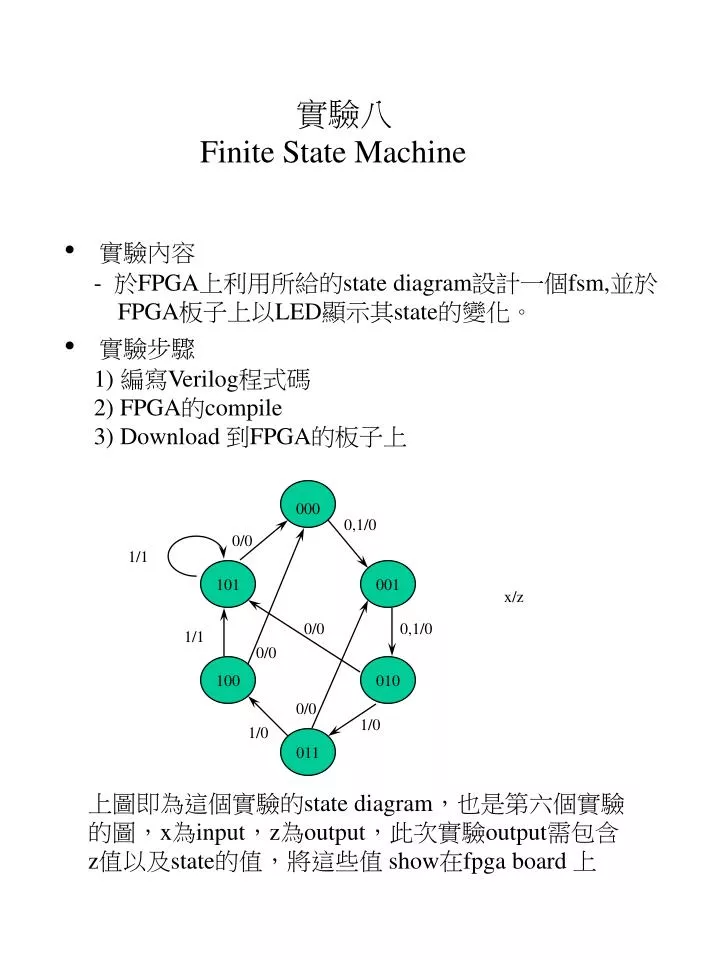
實驗八 Finite State Machine. 實驗內容 - 於 FPGA 上利用所給的 state diagram 設計一個 fsm, 並於 FPGA 板子上以 LED 顯示其 state 的變化。 實驗步驟 1) 編寫 Verilog 程式碼 2) FPGA 的 compile 3) Download 到 FPGA 的板子上. 000. 0,1/0. 0/0. 1/1. 101. 001. x/z. 0/0. 0,1/0. 1/1. 0/0. 100. 010. 0/0. 1/0. 1/0. 011.

E N D
實驗八 Finite State Machine • 實驗內容 • - 於FPGA上利用所給的state diagram設計一個fsm,並於 • FPGA板子上以LED顯示其state的變化。 • 實驗步驟 • 1) 編寫Verilog程式碼 • 2) FPGA的compile • 3) Download 到FPGA的板子上 000 0,1/0 0/0 1/1 101 001 x/z 0/0 0,1/0 1/1 0/0 100 010 0/0 1/0 1/0 011 上圖即為這個實驗的state diagram,也是第六個實驗 的圖,x為input,z為output,此次實驗output需包含 z值以及state的值,將這些值 show在fpga board 上
1) Write verilog program ; 2) Compile verilog program: <1> From ex-7 , we can learn how to initialize the synopsys: - edit .synopsys_dc.setup to setup designer . - command : source synopsys.env - command : design_analyzer , to startup synopsys - when design analyzer appear : Click Setup -> Command to open command window <2> Step of FPGA compiler and download Step1: generating .sxnf file 1.File ->Read->file1.v (your verilog file like fsm.v) 2.Click on the top module 3.Edit->Uniquify->Hierarchy (2,3 can be replace by click the input port twice) 4.Defining input/output ports as pads Attributes -> optimization directives -> input port -> port is pad->Apply ...........................->output port ->port is pad ->Apply 5.Defing clock port as a port Attributes -> optimization directives -> input port -> port is pad -> signal type ->clocked on also ->Apply 6.Type “ insert_pads” in command window 7.Tools -> design optimization -> ok When it was complished ,type “replace_fpga” in command window
8. Extract FSM(extract fsm和specify fsm的動作只須試了後 寫在報告上即可,在板子上不需要經過這兩個動作,也 就是不必經過step8和step9,因此step10也不用做) i.Click your FSM design ii.Click “Tools” ->Finite State Machine->Extract FSM from Netlist ->Define the Legal States,then a window appear iii.You can see some states in “Order Flipflops in State Vector” subwindow and type the following two commands. ->set_fsm_state_vector {“state_reg<2>“ “state_reg<1>”....}, Note that state_reg<*> are your states shown in the subwindow. ->group -fsm -design_name New_Design_Name to assign a new name to the grouped circuits (e.g. fsm2) iv.Click on your “New_Design_Name” like fsm2 and click “OK” 9.Specify FSM encoding Style i.Click “Tools”->Finite State Machines->State Encoding ii.There are four styles including Binary,Gray,One Hot, and Clear All. Different styles make different results. Try to find the best results. iii.Choice one style and click “OK” ->Compile ->OK. iv.Click “TOP”design and type “compile” 10.When 9 was complished , repeat step 7. 11.setting part type ( in command window) typing-> set_attribute designname “part” -type string “4003apc84-5”
12.setting I/O port pin location design (in command window) typing -> set_attribute i/o portname “pad_location” -type string “P#” where # is FPGA pin number 13.File ->save as ->design_name.db (format:db) ->save as ->design name.sxnf(format:xnf) ps.從step11開始也可以用另一種方法來設定part type 以及i/o port pin location <i> 先將檔案save成.db and .sxnf檔 <ii>edit your .sxnf file <in design_name.sxnf> ----------------------------------- .................. PART , 4003apc84-5 <--------here set part type .................. .................. .................. EXT,A,I,,LOC=P19 <--- here set input port A at pin 19 EXT,B,I,,LOC=P20 <----...............................B...........20 EXT,C,O,,LOC=P57 <---..............output.......C...........57 .. ---------------------------------- STEP 2 : generating .bit file (in C shell) (For current version of Synopsys,the default global clock is secondary global clock . If you want to use the primary clock , you have to replace “BUFGS”, with “BUFGP”,in .xnf file.) 1.syn2xnf design_name when 1 was complished that you could get .xnf file
2.source xact.env • 3.xmake design_name.xnf • when 3 was complished ,you could get .bit file • if have errors you can read message from file.out • and file.prp • STEP 3 download (in PC) • xchecker design_name.bit • 以下為板子上的所使用的pin number • Clock使用P13,再利用跳接線,連接P13與SW5(左邊aaaaaa • 第二個按鍵式的switch),pin number為18。 • input x可任選SW3的其中一個使用,pin #如下: State選用下列其中三個LED使用,請各位選連續的 三個使用,其pin # 如下:
PS:這個實驗中板子上面要demo的是不用經過extractPS:這個實驗中板子上面要demo的是不用經過extract • 及specify,但是仍須將此二個步驟跑過,再用 • Cadence-Xilinx Interface的timing simulation netlist • generator去得到*.v和 *.stim(Verilog & stimulus • 檔案),再用Verilog-XL Logic Simulator即可做 • simulation • Cadence-Xilinx Interface存放目錄路徑為: • /usr/cadence/tools/pic/picdesigner/bin • Timing Simulation Netlist Generator • input file: fsm.lca(在做完上述所有動作後即會產生此檔) • output file: fsmt.v fsmt.stim • command: timenet fsm.lca 4000 -r . -x • Verilog Simulation • 產生 Simulation Netlist後,編輯 .stim檔加入test patterns • 直接呼叫Verilog-XL Logic Simulator即可做simulation • command: verilog fsmt.v file fsmt.stim • 由simulation的結果去判斷那個code(binary,grey...)會得到最 • 好的optimize結果,將結果寫在報告上,因此此次實驗需 • 要有不做extract & specify的結果供板子使用和有做extract • &specify的寫在報告上,所有步驟都照上述。