Download
1 / 1
10 likes | 90 Views
半導體元件研究室. The Sixth International Workshop on Junction Technology (IWJT), May 15-16, 2006, Shanghai, China. RBS characterization on the PtSi-based ohmic contacts with n-InP. W en- C hang Huang. Abstract.

E N D
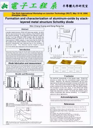
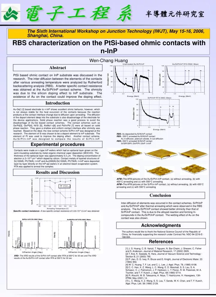
半導體元件研究室 The Sixth International Workshop on Junction Technology (IWJT), May 15-16, 2006, Shanghai, China. RBS characterization on the PtSi-based ohmic contacts with n-InP Wen-Chang Huang Abstract PtSi based ohmic contact on InP substrate was discussed in the research. The inter-diffusion between the elements of the contacts after various annealing temperature were analyzed by Rutherford backscattering analysis (RBS). A better specific contact resistance was obtained at the Au/Si/Pt/InP contact scheme. The ohmicity was due to the silicon doping effect to InP substrate. The existence of Au on the contact could improve the doping effect. Introduction Au-Ge[1,2] based electrode to n-InP shows excellent ohmic behavior, however, which is not always stable for the heat excursion of the contacts because the reaction products at the contact interface change due to diffusion upon annealing. The diffusion of the dopant element deep into the substrate is also disadvantage of the electrode for the device applications. Solid phase reaction was a good process to avoid the disadvantage of Au-Ge based contact schemes. The contact schemes such as Ge/Pd[3], Ge/Pt[4], Ni/Si [5], AlxMo1-x[6] and Pd/In/Pd [7] were all based on solid phase reaction. They gave a shallow and uniform contact interface after ohmicity was reached. Based on the ideal, the new contact scheme Si/Pt/n-InP was designed at the research. The element of Si was chosen to be a dopant element to InP substrate. The element of Pt was used to improve the doping effect. Another contact scheme, Au/Si/Pt/n-InP was designed to compare the results of Si/Pt/n-InP. • RBS– As deposited Au/Si/Ni/InP contact • RBS-- 550C annealed Au/Si/Ni/InP contact • Au in-diffusion, platinum-silicide, In out-diffusion • RBS--550C annealed Si/Ni/InP contact • Si/SiPt/SiPt1.5InP/Pt1.5InP /n-InP Experimental procedures Contacts were made on n-type InP wafers which had an epitaxial layer grown on the semi-insulating substrate by metal organic chemical vapor deposition (MOCVD). The thickness of the epitaxial layer was approximately 0.2 m. The doping concentration of electron is 21018 cm-3 which doped by silicon.Contact metals of layered structures of Si(1300Å)/Pt(750Å)/n-InP and Au(2000Å)/Si(1300Å)/Pt(750Å)/n-InP were deposited layer by layer directly on the InP epi-wafers in an electron-beam evaporation system. RTA was applied to anneal the samples. Results and Discussion AFM--The AFM pictures of the Au/Si/Pt/n-InP contact, (a) without annealing, (b) with 450C annealing and (c) with 550C annealing AFM--The AFM pictures of the Si/Pt/n-InP contact, (a) without annealing, (b) with 450C annealing and (c) with 550C annealing Conclusion Inter-diffusion of elements was occurred in the contact schemes, Si/Pt/InP and Au/Si/Pt/InP after thermal annealing which were observed in the RBS analysis. The Au/Si/Pt/InP contact showed better ohmicity than that of Si/Pt/InP contact. This is due to the alloyed reaction and forming In-compounds in the Au/Si/Pt/InP contact. The wetting effect of Au on the contact was also shown. Specific contact resistance-- A low specific contact resistance of 3.3210-5-cm2 was obtained after RTA at 550C for 30 sec. Acknowledgments The authors would like to thank the National Science Council of the Republic of China, for financially supporting the research under Contract No. NSC-94-2216-E-168-004. References • [1] J. S. Huang, C. B. Vartuli, T. Nguyen, N. Bar-Chaim, J. Shearer, C. Fisher and S. Anderson, Journal of Material Research, 17 (2002) 2929. • [2] T. Arai, K. Sawada, N. Hara, Journal of Vacuum Science and Technology - Section B, 21 (2003) 795. • [3] P. Jian, D. G. Ivey, R. Bruce and G. Knight, Journal of Electronic Mater. 23 (1994) 953. • [4] W. C. Huang, T. F. Lei, and C. L. Lee, J. Appl. Phys. 78, (1995)6108. • [5] C. C. Han, X. Z. Wang, L. C. Wang, E. D. Marshall, S. S. Lau, S. A. Schwarz, C. J. Palmstrom, J. P. Harbison, L. T. Florez, R. M. Potemski, M. A. Tischler, and T. F. Kuech, J. Appl. Phys. 68 (1990) 5714. • [6] R. Atsuchi, M. B. Takeyama, A. Noya, T. Hashizume, H. Hasegawa, 13th IPRM, May (2001) 14. • [7] L. C. Wang, X. Z. Wang, S. S. Lau, T. Sands, W. K. Chan, and T. F. Kuech, Appl. Phys. Lett. 56 (1990) 2129. XRD– The XRD results of the Si/Pt/n-InP contact after RTA at 550C for 30 sec and The XRD results of the Au/Si/Pt/n-InP contact after RTA at 550C for 30 sec