Download
1 / 45
460 likes | 490 Views
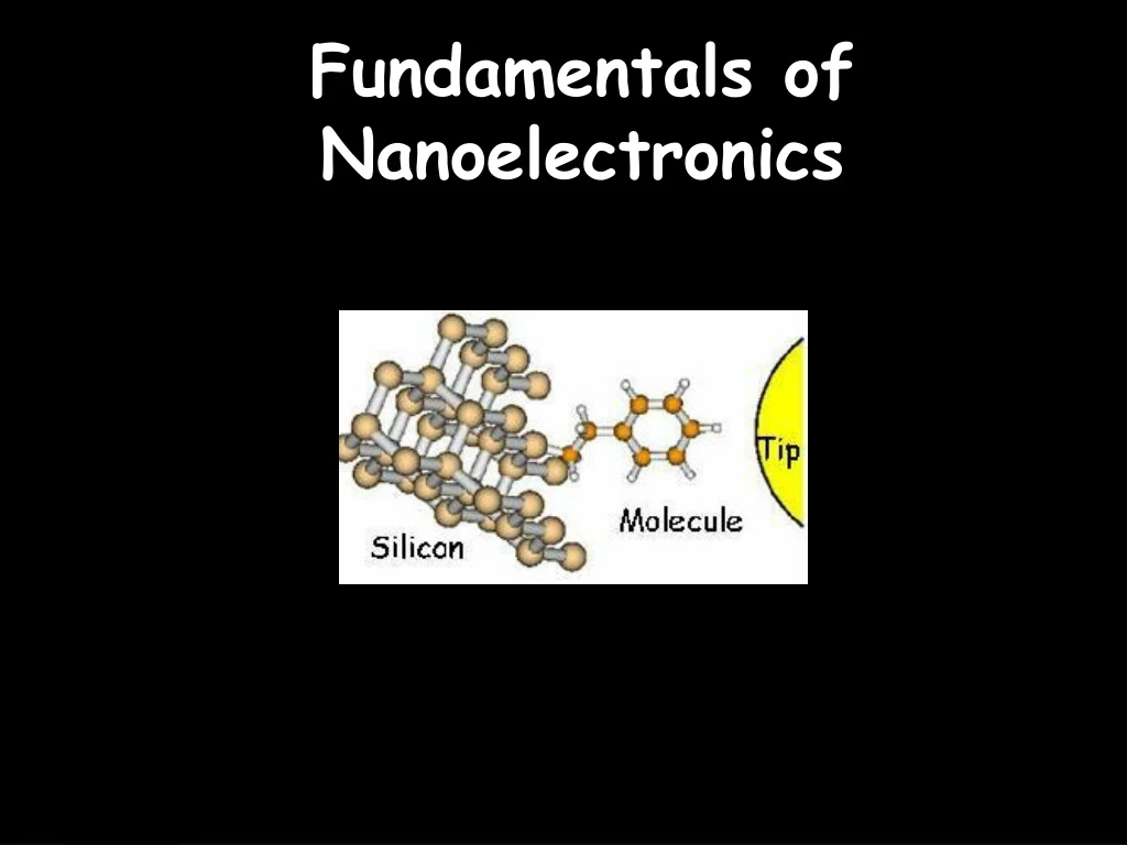
Explore microscopic transport in nanoelectronics, study transistors and quantum effects, and delve into cutting-edge materials and designs for future technology advancement. Learn from Avik Ghosh in this comprehensive course on nanoelectronics.

E N D
ECE 4140/6140 • Instructor: Avik Ghosh (ag7rq@virginia.edu) E315 Thornton (434-243-2347) • Class: MWF 11-11:50 (THND222) • HWs due: F beginning of class • Office hrs/Tutorial: Thursday evenings • Grader: Dincer Unluer (du7x@virginia.edu)Course
General Information on Matlab http://its.virginia.edu/research/matlab/ 1) For students who want to install a copy on their personal computers (need to use the UVAnywhere to start-up Matlab)http://its.virginia.edu/research/matlab/download.html#student 2) For students that want to use the Hive (Virtual Computers with Matlab installed that you can remote login using your personal computer).http://its.virginia.edu/hive/ 3) Use the stack computers.
Course website http://people.virginia.edu/~ag7rq/4140-6140/13/courseweb.html
www.nanohub.org Text/References VIrginia NanOComputing (VINO) http://www.ece.virginia.edu/vino
Syllabus 1st midterm (Feb end) 2nd midterm (Mar end) Final (May start)
Gate Source Drain Channel The Device Researcher’s bread and butter
The Device Researcher’s bread and butter Field effect transistor (FET) Source/Drain Contacts – very conductive Channel – limits resistance of FET Gate – controls resistance of FET
Why study transistors? spin memories Molecular motors open closed ion channel switches (Mackinnon, Nature ’03) Biosensors Many chemical, biological and physical processes involve digital switching with various gates
S-D Current ID Source-Drain Voltage What would we look at in an FET? Saturation S-D Current ID Turn-on Rise Gate Voltage • What’s the physics behind these curves? (HW2) • What about current along z direction?
The driving force behind microelectronics • Moore’s Law: double # FETs/chip in 1.5 years
How far can we scale transistors? New physics emerges at these lengthscales
Cramming more transistors onto a chip • Shorter time for electron to move across channel • More memory elements on a chip • Cheaper
6 nm MOSFET Bruce Doris, IBM 0.7 nm thick MOSFET Uchida, IEDM 2003 Intel’s 2003 transistor Smallness quantum effects Quantum confinement Atomistic fluctuations Leakage, Tunneling Quantum Scattering Silicon transistors already at nanoscale !
A major problem: Power dissipation! (HW1) New physics needed – new kinds of computation
How can we push technology forward?
Better Design Multiple Gates for superior field control (Intel’s Trigate/FinFET)
2 nm SOURCE DRAIN 5 nm Silicon Nanowires (Low m < 100 cm2/Vs) INSULATOR Organic Molecules ? (Reproducibility/ Gateability) Channel VG VD Bottom Gate I Strained Si, SiGe (m ~ 270cm2/Vs) CNTs (m ~ 10,000cm2/Vs) Hard to align into a circuit! < 10 nm Drain Top Gate Source The material ‘zoo’ !! 15 nm
Graphene Atomistic Models Gate Drain Gate Channel Source Architecture Concept Physics Nobel, 2010
Metallic spintronics already exists! GMR (Nobel, 2007) MRAMs Harness electron’s spin “Spintronics” Multiferroics, Nanomagnetism New Principles?
How can we model and design today’s devices?
Pushing the simulation envelope.. Bulk Solid (“macro”) (Classical Drift-Diffusion) Drain ~ 1023 atoms 80s ~ 106 atoms Quantum corrections to classical concepts, usually experimentally motivated (e.g. Quantum Resistance, Quantum interference, etc) Clusters (“meso”) (Semiclassical Boltzmann Transport) Source Channel Bottom Gate Problem: Cannot derive Quantum concepts from Classical equations !!! (e.g. Entanglement in quantum Computation) Today ~ 10-100 atoms Molecules (“nano”) (Quantum Transport)
Bottom-Up instead of Top-Down Bulk Solid (“macro”) (Classical Drift-Diffusion) Drain ~ 1023 atoms 80s ~ 106 atoms Clusters (“meso”) (Semiclassical Boltzmann Transport) Source Channel Bottom Gate Classical Concepts do come out of Quantum Mechanics Phase Breaking Events (“Decoherence”) Today ~ 10-100 atoms Molecules (“nano”) (Quantum Transport)
Bottom-Up instead of Top-Down Bulk Solid (“macro”) (Classical Drift-Diffusion) Clusters (“meso”) (Semiclassical Boltzmann Transport) Classical Concepts do come out of Quantum Mechanics Phase Breaking Events (“Decoherence”) Molecules (“nano”) (Quantum Transport) L > 1 mm L ~ 10 nm L ~ 100s nm source drain
The challenge: Quantum effects = R independent of material, geometry R = h/2q2 = 12.9 kW R < R1 + R2 ! Fano Interference in QDs Ohm’s Law NO MORE! Fourier’s Law NO MORE! RQ independent of material, geometry k = p2kB2T/3h = 0.95pW/K
The challenge: Atomistic effects Nanotube Data Williams group, UVa Characterizing single molecular traps using noise patterns (UCLA)
Back to familiar I-Vs Saturation S-D Current ID S-D Current ID Turn-on Rise Gate Voltage Source-Drain Voltage What does a device engineer look for?
Subthreshold Swing (mV/decade) DIBL (mV/V) Vd=1 S-D Current ID Turn-on Vd=0.5 Gate Voltage Gate Dependence (Transfer Characteristics) VT small to lower power dissipation S small to lower power dissipation (> 60 at room temperature) ON-OFF ratio high (bit error rate in logic) Low OFF current (static power dissipation) DIBL low (OFF current)
Mobility Output conductance S-D Current ID Source-Drain Voltage Drain Dependence Want high mobility (high ON current Faster switching) Want high output impedance (reliability)
How do we understand/model these IVs? Saturation S-D Current ID S-D Current ID Turn-on Rise Gate Voltage Source-Drain Voltage HW2
Starting point: Band-diagram Solids have energy bands (Ch 5) How do we locate the levels?
hn Filled levels Photoemission S + hn S+ + e-
hn Empty levels Inverse Photoemission S + e- S- + hn
hn Level separations Optical absorption S S* + hn
Empty levels Filled levels Semiconductor (Si) (charge movement can be controlled) Metal (Copper) (charges move) Insulator (Silica) (charges can’t move) Filling up the Bands with Electrons E