Download
1 / 34
370 likes | 912 Views
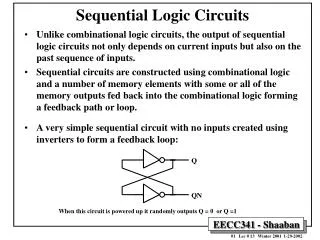
Sequential logic circuits . Outline. Sequential Circuit Models Asynchronous Synchronous Latches Flip-Flops. Sequential logic circuits. The main characteristic of combinational logic circuits is that their output values depend on their present input values.

E N D
Outline • Sequential Circuit Models • Asynchronous • Synchronous • Latches • Flip-Flops Sequential logic circuits
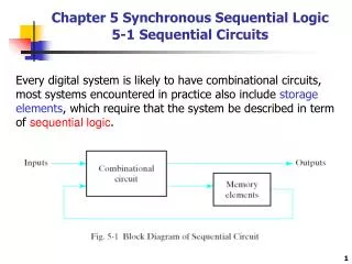
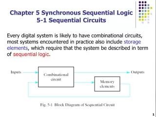
Sequential logic circuits • The main characteristic of combinational logic circuits is that their output values depend on their present input values. • Sequential logic circuits differ from combinational logic circuits because they contain memory elements so that their output values depend on both present and past input values Sequential logic circuits
Sequential logic circuits Sequential circuits can be Asynchronous or synchronous. Asynchronoussequential circuits change their states and output values whenever a change in input values occurs. Synchronoussequential circuits change their states and output values at fixed points of time, i.e. clock signals. Sequential logic circuits
Sequential Circuit Models Universal model Sequential logic circuits
Combinational circuit model Mealy machine model Moore machine model Sequential logic circuits
Sequential Circuit Models Sequential logic circuits
Memory Devices LatchesA latch is a memory element whose excitation signals control the state of the device. A latch has two stages set and reset. Set stage sets the output to 1. Reset stage set the output to 0. Flip-flopsA flip-flop is a memory device that has clock signals control the state of the device. Sequential logic circuits
Latch Flip-flop Sequential logic circuits
Latch and Flip-Flop Devices Sequential logic circuits
Inverter Chains Ring oscillator Sequential logic circuits
Latches RS Latch The RS latch is the basic memory element consists of two cross-coupled NOR gates. It has two input signals, S set signal and R reset signal. It also has two outputs Q and Q'; and two states, a set state when Q = 1 and a reset state when Q = 0 (Q' = 1) Sequential logic circuits
Theoretical state diagram of cross-coupled NOR gates Sequential logic circuits
Observed state diagram of cross-coupled NOR gates Sequential logic circuits
RS Latch excitation table Sequential logic circuits
State, Clock, Setup Time, and Hold Time The Clocking event can be either from low to high or from high to low. The input signal around clocking event must remain unchanged in order to have a correct effect on the outcome of the new state. • Tsu: the minimum time interval preceding the clocking event during the input signal must remain unchanged • Th: the minimum time interval after edge of the clocking event during the input signal must remain unchanged Sequential logic circuits
Timing Diagram of RS-Latch Sequential logic circuits
JK Latch Sequential logic circuits
Level-Sensitive Latches A level-sensitive latch is a latch with an additional enable input. RS latch Sequential logic circuits
RS Latch with Enable Sequential logic circuits
D Latch Q+ = D Sequential logic circuits
Flip-Flops A flip-flop is a level-sensitive latch with a clock input. RS flip-flop Q+ = S +R'Q Sequential logic circuits
T (Toggle) flip-flop Q+ = TQ' + T'Q Sequential logic circuits
Master Slave Flip-Flops A master slaveflip-flop consists of two latches and an inverter. Master-slave RS flip-flop Sequential logic circuits
Master-Slave JK Flip-Flops Sequential logic circuits
Positive Edge-Triggered Flip-Flops Positive edge-triggered RS flip-flop timing diagram Sequential logic circuits
Positive edge-triggered JK flip-flop timing diagram Sequential logic circuits
Positive edge-triggered D flip-flop timing diagram Sequential logic circuits
Positive Edge-Triggered Timing A circuit that generates a positive edge-triggered timing signal can be constructed as follows: Sequential logic circuits
Exercises page 425, 6.1-6.6, 6.9, 6.10, 6.12, 6.13, 6.14, 6.17, 6.24, 6.25 Sequential logic circuits