Download
1 / 12
120 likes | 357 Views
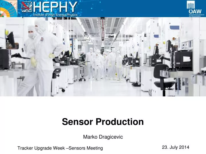
Sensor Production. Tracker Upgrade Week –Sensors Meeting. 2S Sensor (6” version). 2S Prototype. Overview. Main Purpose Produce a full size (6”) 2S sensor to test hybrids, assembly, etc. Side Quest: Test different design options for the sensor Vendor for the production: tbd this week.

E N D
Sensor Production Marko Dragicevic Tracker Upgrade Week –Sensors Meeting
2S Sensor (6” version) Marko Dragicevic
2S Prototype Overview • Main Purpose • Produce a full size (6”) 2S sensor to test hybrids, assembly, etc. • Side Quest: • Test different design options for the sensor • Vendor for the production: tbd this week Marko Dragicevic
2S Prototype Production • CNM: 6” strip production not available before 2016! • CiS: 6” production is new! 200 µm physical thickness could be challenging • Infineon: • Low price quoted is due to sharing of costs for this run • First production of n-on-p sensors • We get 25 wafers, min 10 have to fully comply with our specs rest can be slightly outside • If run is successful, we can order additional pieces for 1000 EUR/wafer (in batches of 10) • * for 25 wafers, min. 10 with full specs Marko Dragicevic
2S Prototype Production • Cheapest, reliable manufacturer is: HPK • Sensors of reliable quality are needed soon to test module components • HPK is an important candidate for the mass production • Suggest to additionally produce with Infineon • Offers possibilities that HPK might not • [O] lean, pure FZ • Test of layout and process optimisations • Production needs to be qualified if we want Infineon for the mass production Marko Dragicevic
2S Prototype Baseline Design 2S Sensor • Wafer: • Wafer diameter (6” wafer): 150 mm • Forbidden margin 5 mm -> 140 mm usable • Sensor • Strips: 1016 (8 x 127) • Strip Pitch: 90 µm • Width/Pitch: ~ 0.25 • P-stop: Atoll, 4 µm width, 6 µm spacing • 2S Sensor size • Fitted size to what is used in CAD models • Not optimised for optimal wafer usage! • Sensor width: 94.183 mm • Sensor length: 102.7mm • Active size: 100.6 x 91.5 mm2 140 mm 5 mm 150 mm 102.7 mm 94.183 mm Marko Dragicevic
2S Prototype Wafer Layout • 2S sensor • 94 mm x 103 mm • Test sensors • 1 x BabyStrip: 127 ch x 50 mm • 6 x BabyStrixel: 127 ch x 23 mm • 4 x TinyStrixel: 127 ch x 12.5 mm • Teststructures • Wafer will be filled with Teststructures • Currently only Diodes are implemented • Size of TS will be significantly reduced compared to old “Halfmoon” TinyStrixel 2S Sensor BabyStrixel BabyStrixel BabyStrip Marko Dragicevic
Design Options • BabyStrip: • Standard test sensors for CBC with 5 cm strips • BabyStrixel • P-stop Atoll geometries • Following the results from the KIT/CNM run • P-stop Common geometries • Consumes less space, should have similar performance • Strixel segmentation area • Optimising the pitch between strixels at the segmentation area • Center Bias Line for strixels • To connect strixels at the center • Moves bond pad nearer to sensor edge • Irradiation Sensor • Standard design like main 2S Sensor Prototype • ??? • TinyStrixel • No P-stop 2. - 4. ??? TinyStrixel 2S Sensor BabyStrixel BabyStrixel BabyStrip Marko Dragicevic
Sensor Layout Bias Ring • Distance to edge (centre of contact area): 1 mm • Width of opening: 110 µm Probe pads • Non-staggered • Size - distance to edge • DCPad: 66 x 118 µm2 - 1.5 mm • ACPad: 66 x 196 µm2 - 1.7 mm Bond pads • Staggered • 4 rows (2 pads on each strip) • Each ACpad 110 x 390 µm2 • Distance to edge • Row 1 (uneven strips): 2.1 mm • Row 2 (uneven strips): 2.6 mm • Row 3 (uneven strips): 3.0 mm • Row 4 (uneven strips): 3.5 mm Marko Dragicevic
Conclusions I The 2S Prototype Sensors are an essential step in the Tracker R&D to successfully: • Evaluate the design of the 2S sensor • Test of different sensor layout options with small sensors • Evaluate radiation hardness of sensor design and material • Continuation of the HPK Thin Sensor Campaign • Evaluate the 2S module design by building a full size prototype • Already needed now to test 8xCBC hybrid prototypes • Evaluate vendors and prepare for the mass production Marko Dragicevic
Conclusions II Upcoming sensors productions (2S, MAPSA-light and 8”) will yield plenty of test sensors and structures! Great opportunity to: • Join the effort to characterise sensors and test structure • Great opportunity to perform interesting studies with your students If you are interested contact • Alexander Dierlamm • Marko Dragicevic Marko Dragicevic