Download
1 / 29
290 likes | 309 Views
Learn about closing the gap between ASIC and custom designs, implementing physical prototyping plans for high performance, overcoming design problems, utilizing physical prototyping techniques for efficient design implementation, and enhancing ASIC performance.

E N D
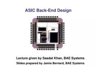
Closing the Gap Between Asic & Custom: Tools and Techniques for High-Performance ASIC Design • Physical Prototyping Plans for High Performance (ch. 6) • Early Planning and Analysis for Area, Timing, Routability, Clocking, Power and Signal Integrity • Automatic Replacement of Flip-Flops by Latches in ASICs (ch.7) • Useful-Skew Clock Synthesis Boosts ASIC Performance (ch. 8) Closing the Gap Between Asic & Custom: Tools and Techniques for High-Performance ASIC Design
Physical Prototyping Plans for High Performance • Introduction • Premise • Current backend tools can only handle local optimization • Front-end and back-end tools are not collaborating • Global optimization not possible, inter-block communication delays known only after full P&R • Design Problem • Slow and inefficient design implementation • Entire synthesis / P&R flow has to be rerun if timing closure is not met • Most likely not all potential of the design will be achieved • Solution: Physical Prototyping Closing the Gap Between Asic & Custom: Tools and Techniques for High-Performance ASIC Design
Physical Prototyping Plans for High Performance • Traditional Floorplanning • Tasks • Determine the shape and location of different blocks • Assign / place pins • Determine block timing budget • Calculate the power grid and clock tree • Goals • Meet timing / area / power constraints • Minimize dead space • Guarantee routability • Minimize total wire length • Problem: lack of physical information • NP-hard problem • Placing the design blocks is more or less a heuristic process • Stochastic methods such as simulated annealing and genetic algorithms are normally used Closing the Gap Between Asic & Custom: Tools and Techniques for High-Performance ASIC Design
Physical Prototyping Plans for High Performance • Physical Prototyping • A physical prototype of the design is quickly created • What-if –experiments can be used to rapidly test different alternatives • Quick logic synthesis • No accurate timing data • Simple wire-load models • Floorplanning • Automatic & interactive placement • Quick physical implementation • Block-level physical synthesis, trial route • In-place optimization • Clock tree synthesis • Physical prototype • Netlist + physical and timing constraints for each block Closing the Gap Between Asic & Custom: Tools and Techniques for High-Performance ASIC Design
Physical Prototyping Plans for High Performance • Physical Prototyping • The partitioning is done on a flat full-chip view • Hierarchical approach is maintained while benefiting from the flat design optimization • Blocks can be even black box designs or high-level RTL code • Individual blocks can be refined until the desired result is achieved • New prototype is generated when a block is implemented • e.g. RTL -> netlist • Accurate timing/area data -> more detailed prototype • After all blocks are finished, the final back-end flow is run Closing the Gap Between Asic & Custom: Tools and Techniques for High-Performance ASIC Design
Physical Prototyping Plans for High Performance • Physical Prototyping • Results • Prototyping flow • Cadence First Encounter 2002.1 • Final back-end flow • Avant! Apollo, Star-RCXT • Synopsys PrimeTime • Mentor Calibre • ”Comparison of the routing, extraction and timing analysis times between the prototyping environment and the traditional back-end implementation tools shows that the productivity gain with quick prototyping in the design cycle is significant.” Closing the Gap Between Asic & Custom: Tools and Techniques for High-Performance ASIC Design
Physical Prototyping Plans for High Performance • Physical Prototyping • Hierarchical approach is imperative, but should be combined with a global perspective • Hierarchical Cadence First Encounter design flow • Flat full-chip prototype model • Timing budget, placement, aspect ratio etc. for blocks • Models of the individual blocks • Optimization • Iterative improvement Closing the Gap Between Asic & Custom: Tools and Techniques for High-Performance ASIC Design
Physical Prototyping Plans for High Performance • Techniques in Physical Prototyping • Blocks do not need to be rectangular • irregular shapes allow more flexible placement and more efficient area use • Physical locality is achieved by utilizing logical hierarchy • Intra-block routing 95% • Inter-block routing 5% • Optimization focus on the bottleneck inter-block signals • Changes can be made locally without breaking the integrity of the entire design • e.g. cells can be re-sized or replaced with complex cells • Pin assignment integrated to global routing • Trial route • Fast execution, no DRCs • Priority to global routing Closing the Gap Between Asic & Custom: Tools and Techniques for High-Performance ASIC Design
Physical Prototyping Plans for High Performance • Techniques in Physical Prototyping • Power planning flow • Semi-automatic • Power grid/rings • Prototype • Parasitics • Power analysis • Iteration Closing the Gap Between Asic & Custom: Tools and Techniques for High-Performance ASIC Design
Physical Prototyping Plans for High Performance • Conclusions • Traditional floorplanning does not consider the DSM physical effects • Physical prototyping provides a playground where design trade-offs can be experimented with • Design constraints are constantly monitored and verified • The prototype can be refined incrementally • Physical prototyping helps partitioning into manageable blocks • Hierarchical design methodology • Realistic block-level timing budgets • The Physical prototyping tool covers: • Partitioning • Generation of block-level –constraints • Top-level design closure • Clock tree synthesis • Power grid design Closing the Gap Between Asic & Custom: Tools and Techniques for High-Performance ASIC Design
Physical Prototyping Plans for High Performance • Comments • Significant advances in EDA tools during the last 5 years • Especially back-end and verification tools have been improved • There are companies that provide a complete flow from design entry to tapeout • Most likely these flows feature co-operation b/w front-end and back-end tools • “Front-end logic designers resist engaging in physical design issues.” • Current state of the art was not researched At least the proposed physical prototyping should not make the functional verification more difficult Closing the Gap Between Asic & Custom: Tools and Techniques for High-Performance ASIC Design
Automatic Replacement of Flip-Flops by Latches in ASICs • Introduction / Motivation • Latches vs. Flip-Flops • Latches are smaller than FFs • Latches are somewhat immune to clock skew • FFs (single-phase) are immune to duty cycle jitter • Latches allow slack passing / time borrowing • In FF-based designs, the slowest pipeline stage always determines the clock period • Verification of latches (both timing and functional) is anything but trivial • Very limited support in EDA tools Closing the Gap Between Asic & Custom: Tools and Techniques for High-Performance ASIC Design
Automatic Replacement of Flip-Flops by Latches in ASICs • Initial design: only flip-flops, clock period T • Identify FFs to be replaced • Determine input and output timing constraints to ensure optimal latch positions • Replace each FF with two FFs • Clock period -> T/2 Automatic Replacement of Flip-Flops with Latches Closing the Gap Between Asic & Custom: Tools and Techniques for High-Performance ASIC Design
Automatic Replacement of Flip-Flops by Latches in ASICs • Perform retiming / delay balancing • The created new pipeline stages must run at twice the original speed • Synthesis tools support retiming in FF-based designs • Replace the retimed FFs with latches of clock period T • Resize gates to benefit from the time savings • FF setup time, clock skew Automatic Replacement of Flip-Flops with Latches Closing the Gap Between Asic & Custom: Tools and Techniques for High-Performance ASIC Design
Automatic Replacement of Flip-Flops by Latches in ASICs • Equivalent Circuits • A sequential path with n FFs is equivalent to a sequential path with 2n latches (corollary!) • Active-low latches followed by active-high latches • Proof: see book Closing the Gap Between Asic & Custom: Tools and Techniques for High-Performance ASIC Design
Automatic Replacement of Flip-Flops by Latches in ASICs • Restrictions • In some cases replacing FFs with latches is impossible or unfeasible • Single-cycle loops • Slack passing not possible -> FF-based design is faster • Single-cycle blocks with ninputs , noutputs << ninternal_signals • The amount of needed latches can grow rapidly • Designs with gated clocks, multi-cycle paths, multiple-clock designs • The latch inputs should arrive when the latches are transparent, not at the clock edges • Preferably in the middle of the clock edges • The effect of clock skew and jitter are minimized Closing the Gap Between Asic & Custom: Tools and Techniques for High-Performance ASIC Design
Automatic Replacement of Flip-Flops by Latches in ASICs • Each latch separated by T/2 • The delay for the first stage is 3T/4 – c (input constraint) • The delay for the last stage is 3T/4 – d (output constraint) • Note: if the doubled FFs are not moved in the retiming, the pipeline delay was less than T/2 -> the original FFs should be reinstated Optimal Latch Positions Closing the Gap Between Asic & Custom: Tools and Techniques for High-Performance ASIC Design
Automatic Replacement of Flip-Flops by Latches in ASICs • Results • Synthesizable 32-bit embedded processor, 0.13mm SC CMOS, Synopsys DC/PC 2000.11-SP1, PrimeTime, Cadence Silicon Ensemble, Pearl • Latch based designs 6-19% faster, 3-11% larger • Floorplanning and routing took 4x the FF-design time • Functional verification was not possible Synthesis results Post-physical compiler results Closing the Gap Between Asic & Custom: Tools and Techniques for High-Performance ASIC Design
Automatic Replacement of Flip-Flops by Latches in ASICs • Conclusions • Some critical path delay improvement can be achieved by replacing the flip-flops of an ASIC design by latches • Small area penalty as a drawback • Automatic replacement using scripts and synthesis tools is possible • The process consists of: • Identifying the FFs to be replaced • Replacing each FF with two FFs of half clock period • Performing retiming / delay balancing • Replacing retimed FFs with latches of clock period T • Resizing gates to benefit from the time savings Closing the Gap Between Asic & Custom: Tools and Techniques for High-Performance ASIC Design
Automatic Replacement of Flip-Flops by Latches in ASICs • Comments • Accurate functional verification and scan-type structures are most likely unthinkable with the latch-based designs • Then again, it it possible that the verification could be done with the initial FF-based design, and the latch-conversion performed thereafter The achievable speed gains will probably be smaller with more control-oriented designs • All the results were obtained from the optimizations of a 32-bit embedded processor The effect on power consumption was not even mentioned Closing the Gap Between Asic & Custom: Tools and Techniques for High-Performance ASIC Design
Useful-Skew Clock Synthesis Boosts ASIC Performance • Introduction • Clock skew is generally considered very harmful • Design verification (both timing and functional) is more difficult with skewed clocks • Synthesis tools aim at minimizing the clock skew • Heavy buffering • High-priority routing Some controlled and intentional clock skew can however: • Reduce power consumption • Reduce switching noise • Improve speed • Clock skew is normally utilized only in custom designs Closing the Gap Between Asic & Custom: Tools and Techniques for High-Performance ASIC Design
Useful-Skew Clock Synthesis Boosts ASIC Performance • Example 1: Increasing Clock Frequency • Two pipeline stages, 1st stage delay 2ns, 2nd stage delay 6ns • Zero-skew -> f = 167MHz • 2ns positive skew -> f = 250MHz (clock period = 4ns) • Allowing / generating the clock skew yields similar time borrowing between successive pipeline stages as with latch-based designs Closing the Gap Between Asic & Custom: Tools and Techniques for High-Performance ASIC Design
Useful-Skew Clock Synthesis Boosts ASIC Performance • Example 2: Increasing Safety Margins • Two pipeline stages, 1st stage delay 1…3ns, 2nd stage delay 5…8.5ns, clock period 9.0ns • Zero-skew -> safety margin 1.0/0.5ns • 2ns positive skew -> safety margin 3.0/2.5ns • Allowing / generating the clock skew is used to widen the safety margins in order to avoid possible race situations Closing the Gap Between Asic & Custom: Tools and Techniques for High-Performance ASIC Design
Useful-Skew Clock Synthesis Boosts ASIC Performance • Permissible Skew Range • Clock skew must always be within certain limits • Too small skew will cause a race condition • Skew must be larger than the hold time – the shortest path delay • Too large skew will cause a cycle time violation • Skew must be smaller than the clock cycle – the longest path delay – setup time Closing the Gap Between Asic & Custom: Tools and Techniques for High-Performance ASIC Design
Useful-Skew Clock Synthesis Boosts ASIC Performance • Zero-Skew Problems • High peak current and switching noise • All flip-flops switch at the same time -> massive current peaks • Non-zero skew alleviates these problems • The flip-flop switching current is divided into a longer time interval Closing the Gap Between Asic & Custom: Tools and Techniques for High-Performance ASIC Design
Useful-Skew Clock Synthesis Boosts ASIC Performance • Useful-Skew Design Flow • First, the traditional zero-skew design flow is run Closing the Gap Between Asic & Custom: Tools and Techniques for High-Performance ASIC Design
Useful-Skew Clock Synthesis Boosts ASIC Performance • Useful-Skew Design Flow • Next, clock skew is applied to the design • Automatic useful-skew tool: Celestry ClockWise • Skew optimization steps: • Permissible range generation • Min/max skew for adjacent FFs • Initial skew scheduling • Best schedule chosen • Clock tree topology synthesis • Buffer tree • Clock net routing • Clock timing verification Closing the Gap Between Asic & Custom: Tools and Techniques for High-Performance ASIC Design
Useful-Skew Clock Synthesis Boosts ASIC Performance • Results and Conclusions • Slack improvement said to be typically 5-15% of the clock cycle • Example: a graphics chip • The useful-skew optimization should be combined with cell/gate (re)sizing • Cell/gate sizing trades area for improved delay • Cell/gate output transistors are grown to increase the current drive • Skew optimization can create more timing slack to avoid high area penalties of cell/gate sizing Clock skew can be used to • Reduce power consumption / peak currents • Reduce switching noise • Improve speed / increase safety margins / help reaching timing closure Closing the Gap Between Asic & Custom: Tools and Techniques for High-Performance ASIC Design
Useful-Skew Clock Synthesis Boosts ASIC Performance • Comments • The effect on current peaks and switching noise is probably more beneficial than the possible speed gains • Timing verification will become interesting as the number of different-phase clock domains explodes • Apparently only buffers are used in creating both positive and negative clock skews Closing the Gap Between Asic & Custom: Tools and Techniques for High-Performance ASIC Design