Download
1 / 12
120 likes | 283 Views
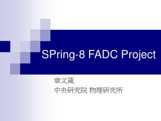
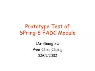
Prototype Test of SPring-8 FADC Module. http://www.rcnp.osaka-u.ac.jp/~wchang/LEPS /PrototypeTest_FADC_SP8.ppt. SPring-8 FADC Module (4 channels, 10 bits, 40 MHz). FIFO. FADC. OPA. FPGA. Mixed signal AD Converter Adapter Board. 40 MHz sampling rate.

E N D
Prototype Test of SPring-8 FADC Module http://www.rcnp.osaka-u.ac.jp/~wchang/LEPS /PrototypeTest_FADC_SP8.ppt
SPring-8 FADC Module(4 channels, 10 bits, 40 MHz) FIFO FADC OPA FPGA
Mixed signal AD Converter Adapter Board • 40 MHz sampling rate. • 10 bits resolution with 2Vp-p dynamic range. • Clock distribution with Phase Lock Loop circuit. • On Board digital signal delay and • Real-Time ZERO-Suppression. • High capacity First In First Out Memory. • Easy to use with high density connector.
FADC Mother Board Driver CPLD Clock Driver VME Connector
VMEBus slave controller, with high performance BLTransfer Mode. FPGA, digital signal control chip. First In First Out memory. Differential AD Converter (40 MHz) 16 channels differential signal input connector. 32 Channels, high sampling rate Flash AD converter. Spring-8 2002/03
CS: Checksum bit Data Format Lowest Bit ND: Not defined. Header ADC Time Trailer We need a place for Event Counter.
FADC VME Action List (A24/D16) • 0x0i0000: address to write, bit 9 for resetting FIFO, bit 10 for resetting suppression threshold and 10 bits for setting the sample count of the FADC i. (Address modifier: 0x3D). • 0x0i0100: address to read the merged 32 FIFOs’ content in BLT mode for FADC i. (Address modifier: 0x3B, 0x3F). • 0x0i0101: address to read the BLT reading cycle for FADC i. (Address modifier: 0x3B, 0x3F). • 0x0i0000+j*0x000100: address to read the single FIFO content in AO mode for channel j. (Address modifier: 0x3D) • 0x0i0000+j*0x000100: address to write for setting the zero-suppression threshold for channel j. (Address modifier: 0x3D)
The Control Flow of FADC For each channel DAQ Start Trigger , Conversion Master Yes NIM < 5 events Preamplifier Module VME CPU No Trigger Count *Veto Send IRQ to VME CPU Trigger signal DAQ READ FIFO CPLD FADC Trigger Clock 100MHz DAQ send Reset FADC Module Trigger FADC set ready FADC Reset Clear trigger Veto Clear Slave
Observation Window of Signals Signal Shift Register Length (2.5 s) Trigger Conversion Strobe Sampling Counts (1024*25ns=25s)
To-do Itmes During SPring-8 Visit • Complete one full 32-channel FADC module. • TEXONO DAQ. • Finalize and implement the VME action list. • Determine and implement the default values for shift register length (1-2 micro sec) and sampling count (about 600). • Implement the functions of “Reset” and “Busy” on the front-panel Lemo inputs and the definition of LED lights. • Fix up the gain range and signal coupling on the analog input. • Fix up the scheme of defining FADC reference voltage (pedestal) and zero suppression threshold.
Things to do after SPring-8 visit • Finish up another 32-channel FADC module and ship it for use by the end of March. • Prototype 2 before the final production?? • Get the feedback and finalize the layout and part lists for FADC modules. • Issue out the purchase orders of electronic parts and board fabrication by 04/15. FADC Schedule: http://www.rcnp.osaka-u.ac.jp/~wchang/LEPS/FADC_schedule.xls