Download
1 / 19
190 likes | 370 Views
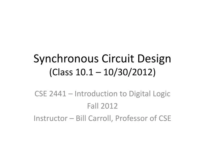
Synchronous Circuit Design ( Class 10.1 – 10/30/2012). CSE 2441 – Introduction to Digital Logic Fall 2012 Instructor – Bill Carroll, Professor of CSE. Today’s Topics. Design of synchronous sequential circuits Lab 8 prelab design exercise.

E N D
Synchronous Circuit Design(Class 10.1 – 10/30/2012) CSE 2441 – Introduction to Digital Logic Fall 2012 Instructor – Bill Carroll, Professor of CSE
Today’s Topics • Design of synchronous sequential circuits • Lab 8 prelab design exercise
Introduction to Synchronous Circuit Design (Synthesis) • Given the circuit requirements (specifications), i.e., word description, state diagram, state table, etc. • Find a hardware realization of the circuit.
Introductory Design Example(from example 8.6, figure 8.21) Given the following state diagram and state table. Derive a circuit realization. Assume D flip-flops will be used for memory. State Diagram State Table
Generate the Transition Table State Assignment State Table Transition Table (Binary state table) (How many flip-flops are needed?)
Produce the Logic Equations Transition Table (Binary state table) Output K-map Flip-flop Excitation (input) K-maps z = xy1’y2 + x’y1y2’ D1= y1y2’ + xy2 D2 = x’y1 + xy1’
Realize the Logic Equations with Gates and Flip-flops z = xy1’y2 + x’y1y2’ D1= y1y2’ + xy2 D2 = x’y1 + xy1’
Lab 8 Preview Analyze, design and implement finite state machines (FSM) • Prelab • Use Quartus/Qsim to analyze a given synchronous circuit (FSM A) • Design a realization of a second circuit (FSM B) given it’s state diagram. • Use Quartus/Qsim to verify the design from 2 is correct. • In lab • Construct and test FSM A on the IDL 800 • Construct and test FSM B on the DE1
Test Your Understanding (Lab 8, Prelab 2) Design a realization of the following state diagram. Use D flip flops as memory.
Test Your Understanding – Self-Check Given the state diagram. Construct a state table. A B C D Construct Excitation Table For D flip-flops, transition tables and excitation tables are the same with D1=Y1 and D2 = Y2. Construct a Transition/Output Table Y1Y2
Test Your Understanding – Self-Check Construct Excitation Maps Generate logic equations for D1, D2, z1, and z2 D1 = x’y2 D2 = x + y1’y2 z1 = y1 z2= y2 D1 D2
Test Your Understanding – Self-Check Realize the logic equations with gates and flip flops
Using JK Flip Flops as Memory for Figure 8.2 (Example 8.7) Figure 8.23 J1 = xy2 K1 = x’y2 J2 = xy1’ + x’y1 K2 = xy1 + x’y1’
Clocked JK Flip-Flop Implementation (Example 8.7) Figure 8.24 J1 = xy2 K1 = x’y2 J2 = xy1’ + x’y1 K2 = xy1 + x’y1’
Test Your Understanding Design a realization of the following state diagram. Use JK flip flops as memory.
Test Your Understanding – Self-Check Given the state diagram. Construct a state table. A B C D Construct Excitation Tables Construct a Transition/Output Table Y1Y2 J2K2 J1K1
Test Your Understanding – Self-Check Construct Excitation Maps Generate logic equations for J1, K1, J2, K2, z1, and z2 J1= x’y2 K1= x + y2’ J2 = x K2 = x’y1 z1= y1 z2= y2 J1 K1 J2 K2
Test Your Understanding – Self-Check Realize the logic equations with gates and flip flops
Synchronous Circuit Design (Synthesis) • Step 1 – Given a description (specification) of the circuit requirements, derive a state table that meets the requirements. Often it’s easier to first derive a state diagram followed by the equivalent state table. • Step 2 – Find a state table with a minimum number of states that is equivalent to the original state diagram. • Step 3 – Choose a state assignment and generate the state and output transition tables. • Step 4 – Determine (select) the memory device or flip-flop type to be used and find the flip-flop excitation maps. • Step 5 – From the excitation maps, produce (derive) logic equations for the flip-flop inputs. Also, form output maps and produce (derive) the output logic equations. • Step 6 – Draw the logic circuit using the logic equations and appropriate logic devices (gates and flip-flops).