Download
1 / 12
120 likes | 259 Views
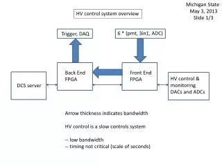
LAr Back End Read Out . Mostly from TDR and updates, but a few additional comments along the way (not specifically LAr ). LAr System Block Diagram. Baseline: “High Speed Links = XAUI” but could change (e.g. PCIe ). Features and Comments: I. Important items shown in block diagram

E N D
LAr Back End Read Out Mostly from TDR and updates, but a few additional comments along the way (not specifically LAr)
LAr System Block Diagram Baseline: “High Speed Links = XAUI” but could change (e.g. PCIe) nSW Meeting (Hobbs/Schamberger/Johns)
Features and Comments: I • Important items shown in block diagram • Carrier + 4 AMC sites (full width AMC) • AMC: • All sites have identical signals • 48 channels 10 Gbps optical Rx/Tx through AMC front panel • XAUI (default), GBT and GbE to carrier • FPGA (see later page) • 2 LVDS Tx/Rx ports as back up path for decoded TTC information • ATCA • 1x (3x?) GBT to each AMC and 4x (8x) GBT to Zone 3 or RTM • XAUI (base line) to AMC and back plane (fabric), but through FPGA • GbE to AMC and back plane (switch, FM2112; or maybe via FPGA) • LVDS (2 ports = 4 differential pairs = 8 single ended signals) • FPGA • Uses Annecy IPMC controller (have test board) nSW Meeting (Hobbs/Schamberger/Johns)
Features and Comments: II • All LAr trigger system communication through GBT and FELIX. • Could ATCA be adapted to handle TTC. Maybe. • May use RTM, and this could be customized for TTC? This was the original plan for transition period • System responsibilities • AMC • optical I/O system: AZ (f/w), BNL (h/w), SBU (h/w) • Final AMC design, Annecy • ATCA • SBU (h/w), AZ (f/w) • Use Annecy IPMC nSW Meeting (Hobbs/Schamberger/Johns)
Features and Comments: III • AMC • OTC: BNL/SBU/AZ developed an AMC card to fully test the optical I/O system. • In practice, added the few features to have a fully functional card • Xilinx Virtex-7 (XC7VX485T-2FFG1927C). Pin compatible w/550, 690 • Connectivity: • Front panel 48 Rx, 48 Tx (micropod) • ATCA connector: XAUI, GbE, 2 full duplex LVDS ports (4 pairs), and two clocks (e.g. ATLAS 40.079 MHz and XAUI clock) • On board clocks: • 125 Mhz (GbE, system clock) • 156.25 Mhz (XAUI) • 40.079 Mhz • CDCM6208 generator fed from either 40.079 on board or one “connector clock” • On board DDR3 memory: 1 GB. Tested at 800 Mhz, rated higher… • Final AMC design by Annecy. Likely an AlteraArria10 FPGA. nSW Meeting (Hobbs/Schamberger/Johns)
Optical Test Card (OTC) • Have v1 prototype. Basically fine. • Demonstrated I/O to 10.3 Gbps on all 48 channels. • >1 day with no errors. Eye approximately 35% open. • This is the rated speed of components • Testing so far • MicroTCA crate (SBU) • Beginning tests in Jumpgen carrier/cpu (AZ; SBU later) • Simple f/w (microblaze) to validate GbE, I2C, • Tested XAUI connections via eye diagram. Full tests need Jumpgen or other carrier. • AZ working on full algorithm f/w nSW Meeting (Hobbs/Schamberger/Johns)
Optical Test Card nSW Meeting (Hobbs/Schamberger/Johns)
OTC, v1 nSW Meeting (Hobbs/Schamberger/Johns)
Optical Test Card (OTC) • v2 boards imminent • Minor changes w/rt v1. • Plan is to make 10 boards (4 SBU, 4 AZ, 2 BNL) • 2 boards with higher speed (13 Gbps) components • About to order FPGAs. Other parts ordered. More than 10? • Unless plans change, this is the last of the OTC production • Proven the I/O system, our job for ATLAS • Expected to be capable of full BE job if needed • Reminder: production version by Annecy (v1, early 2015) probably using Altera nSW Meeting (Hobbs/Schamberger/Johns)
ATCA Carrier • Design and prototyping ongoing • Started w/Annecy design for ATCA infrastructure • Modifications for AMC sites and connectivity • Power increased to ATCA maximum 400 W • Paused to make an eval board for possible ethernet switch • Schematic essentially done. Layout proceeding. September tests • Will use Xilinx FPGA exactly as in the OTC • All design pieces at schematic level for v1 complete • Need to integrate FPGA and switch (if used) into ATCA schematic • Prototype v1 first half of next year nSW Meeting (Hobbs/Schamberger/Johns)
ATCA carrier • RTM or direct to Zone 3 GBT? • Either will use SFP for GBT connection • Depends on: (1) space, (2) I/O ease of access, … • If RTM needed, will be “dumb” RTM ala ATCA spec • Original planning would have dual purpose TTC/s-link or GBT RTMs • May also include GbE switch chip (space and lowest speed) • FPGA primarily for formatting and I/O, but could include some algorithms if useful. • Any other features? nSW Meeting (Hobbs/Schamberger/Johns)
Summary • LAr back end based on AMC + ATCA • AMC • 48 Tx/Rx channels of micropod and clocks on board • XAUI, GbE, GBT, additional clocks via ATCA • Prototype for optical testing, OTC, in hand (Xilinx) • Final AMC version from Annecy (Altera?) • ATCA carrier • Specifications largely in hand • All schematic pieces in hand. Need to put FPGA, enet in main schematic (already has ATCA infrastructure, etc) • 1st prototype early next year nSW Meeting (Hobbs/Schamberger/Johns)