Download
1 / 64
650 likes | 804 Views
Device-level vacuum-packaged infrared sensors on flexible substrates. Aamer Mahmood Advisor: Prof. Donald P. Butler Microsensors Laboratory Department of Electrical Engineering University of Texas at Arlington Arlington, TX 76019. Outline. Introduction MEMS

E N D
Device-level vacuum-packaged infrared sensors on flexible substrates Aamer Mahmood Advisor: Prof. Donald P. Butler Microsensors Laboratory Department of Electrical Engineering University of Texas at Arlington Arlington, TX 76019
Outline • Introduction • MEMS • Infrared radiation and detection • Bolometers • Flexible substrates • Bolometers on flexible substrates • Device-level vacuum-packaged microbolometers • Fabry Perot cavity based tunable infrared microspectrometer
Microelectromechanical Systems (MEMS) • Micro-Electro-Mechanical Systems (MEMS) is the integration of mechanical elements, sensors, actuators, and electronics on a common substrate through microfabrication technology.
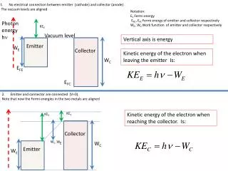
Infrared Detectors • Photon Detectors • Incident radiation generates photo carriers • Photovoltaic detectors • Photoconductive detectors • Photoemissive detectors • Thermal Detectors • Incident radiation causes change in temperature that causes a change in a detector property e.g. • Bolometers (change in temperature causes the detector resistance to change) • Pyroelectric detectors (change in temperature causes the detector capacitance to change) • Thermocouples (use Seebeck effect)
amp I Rb Rb V amp R Bolometers and IR detection • Temperature induces a change in the detector resistance η = absorptivity, = angular frequency of incident radiation, τ = detector thermal time constant, Psignal = the magnitude of the incident flux fluctuation
Bolometer Figures of Merit Temperature coefficient of resistance Normalized change in resistance w.r.t. temperature Responsivity Output/Input
BolometerFigures of Merit Detectivity • Signal-to-noise ratio normalized to the detector area and frequency bandwidth
Flexible substrates • Polyester and Polyimide used as flexible substrates • Polyimide is thermally stable • Polyimide has a Tg of ~400°C • Polyimide is chemically resistant to most clean room etchants • http://www-ee.uta.edu/zbutler/Smart_skin_for_web.ppt
Flexible systems • Advantages of flexible substrate micro sensors • Low cost • Lightweight • Conformable to non planar surfaces • Software based printed IC processes • High degree of redundancy
Flexible systems • Flexible electronics for personal communication (flexible electronic paper) • Smart clothing (Wireless communications with smart sensors and actuators in the ambient) • BioMEMS (flexible electrodes for neural prostheses, vision prosthesis) • Conductive polymers (compound eye, piezoresistive strain sensors) • Flexible energy sources (photovoltaic cells, organic solar cells)
Sensors on flexible substrates (Smart Skin) • Sensor Arrays on flexible substrates • Infrared sensors • Pressure/Tactile Sensors • Flow sensors • Humidity sensors • Velocity sensors
Evolution of “smart skin” in the micro sensors lab • First generation (2001-2002) • Used solid Kapton sheets pasted on to wafers • Second generation (2003-2004) • Spin on Kapton used (no micromachining, not separated from carrier wafer) • Third generation (2004) • Spin on Kapton used (micromachined devices, peeled off carrier wafer) • Fourth generation (2005) • Vacuum packaging at the device level
Microbolometer FabricationTrench Geometry YBCO Au Ti SrTiO3 Si3N4 PI2610 Al SrTiO3 Si3N4 PI5878 Si
Conclusion • Microbolometers on flexible substrates have been fabricated • Mean measured thermal conductance = 5.61x10⁻⁷ W/K • Max room temperature responsivity RV = 7.4x10³ V/W • Max room temperature detectivity D*= 6.6x10⁵ cmHz1/2/W • Measured room temperature TCR = -2.63%/K • Measured room temperature resistance = 3.76MΩ
Device-level vacuum packaging OTMS Si3N4 YBCO Au Ti PI2610 Al SrTiO3 Si3N4 PI5878 Si
Device-level vacuum packaging Optical Window Detector Al Mirror Bond Pad
Device-level vacuum packaging Design Considerations • Optical window transmission characteristics • Optical window structural analyses • Cavity vacuum • Thermal analyses
Optical Transmission Characteristics Transmission characteristics of thin Aluminum Oxide film M. Aguilar-Frutis, M. Garcia, C. Falcony, G. Plesch and S. Jimenez-Sandoval, “A study of the dielectric characteristics of aluminum oxide thin films deposited by spray pyrolysis from Al(acac)3,” Thin Solid Films, vol 389, Issues 1-2, pp 200-206, 15 June 2001.
Structural analysis of vacuum element • Mechanical Strength • Ceramic Al2O3 has a tensile strength of 260 MPa • ZnSe has an apparent elastic limit of 55.1 MPa
Permeability is the flow rate through a specimen once steady state has been achieved He Permeability through Al2O3 at room temperature is ~100-1000 atoms/s/cm/atm n=number of moles R=universal gas constant=8.314J/(mole.K) Permeability through Al2O3
Heat source ((300+ΔT)K) Au Au Au Ti patch Ti patch Si3N4 Si3N4 Si3N4 Top air Ti arm Si3N4 Lower air Al2O3 Si3N4 PI2610 Al2O3 Al2O3 Lower air GA GB GC GD GE GF GG Heat sink (300K) Complete micromachining Incomplete micromachining Ruptured cavity Thermal analysis (analytic)
Thermal analysis (numeric) Gth ≈ 5x10⁻⁶ W/K (Vacuum) ≈10-4 W/K (air)
Microbolometer fabrication Trench Geometry (Not to scale)