Download
1 / 13
130 likes | 340 Views
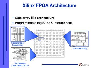
The New FPGA Architecture by Applying The CS-Box Structure. Zhou Lin, Catherine October 13, 2003. Outline. Introduction to the Xilinx FPGA architecture Introduction to the CS-box structure Preliminaries The connection way of pad pins and wire segments.

E N D
The New FPGA Architecture by Applying The CS-Box Structure Zhou Lin, Catherine October 13, 2003
Outline • Introduction to the Xilinx FPGA architecture • Introduction to the CS-box structure • Preliminaries • The connection way of pad pins and wire segments. • The connection way of logic block pins and wire segments.
Outline • Experimental results • Channel width • Routing area • Future work
Basedon the Xilinx FPGA architecture. Combines the connection box and the switch box to form the connection-switch box (CS-box). Introduction to The CS-Box Structure L L CS L L
Introduction to The CS-Box Structure (cont’) • Two types of switches in the CS-box • Those connecting one wire segment to another. • They are set in the same way as in the switch box in the Xilinx FPGA. • Those connecting one pin to one wire segment or vice versa. • The way to set them is the main topic in our research.
Introduction to The CS-Box Structure (cont’) • Two types of CS-boxes • Containing the switches that connect pad pins to wire segments or vice versa. • Containing the switches that connect logic block pins to wire segments or vice versa.
Introduction to The CS-Box Structure (cont’) • Preliminaries • W: Channel width. The number of wire segments in one channel. • Fc_pad: The number of wire segments each pad pin can be connected to. • Fc_input: The number of wire segments each input logic pin can be connected to. • Fc_output: The number of wire segments each output logic pin can be connected to. • P: The number of non-global pins on each logic block or pad.
Fc_pad = W for i:=1 to Fc_pad if iis even Set on the switch connecting the pin to the ith track in the x-directed channel. else Set on the switch connecting the pin to the ith track in they-directed channel. endfor The Connection Way of Pad Pins and Wire Segments 1 L 2 0 Pad L
if W mod P = 0 flag = 0; else m = W / P; flag = 1; for i:=1 to P Connect the pin to the tracks with the number ki, where k=1, 2, …, m; if flag=1 Connect the pin to the track with the number [(m+1)i-W]; endfor The Connection Way of Logic Block Pins and Wire Segments 2 CS 2 2 L i=2 W = 3 & P = 2 m = 1 & flag = 1 i = 2
Future • Do more experiments • Set Fc_pad, Fc_input and Fc_output equal to W / 2. • Apply different switch box structures into the FPGA with CS-boxes.