Download
1 / 56
620 likes | 875 Views
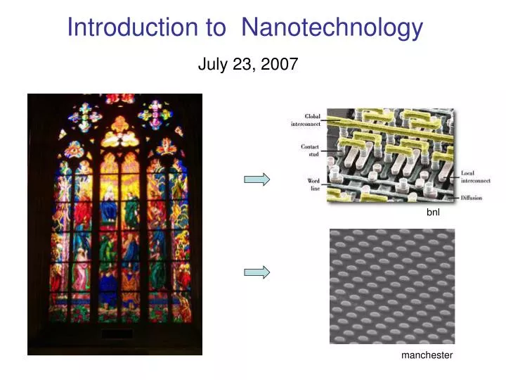
Introduction to Nanotechnology. July 23, 2007. bnl. manchester. Introduction to Nanotechnology. Some things we will discuss:. July 23, 2007. How big are nanostructures Scaling down to the nanoscale How are nanostructures made? Fabrication, synthesis, manufacturing

E N D
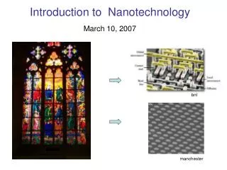
Introduction to Nanotechnology July 23, 2007 bnl manchester
Introduction to Nanotechnology Some things we will discuss: July 23, 2007 • How big are nanostructures Scaling down to the nanoscale • How are nanostructures made? Fabrication, synthesis, manufacturing • How do we see them? Imaging and property characterization (measurement) • Why do we care? Applications to science, technology and society
Why do we want to make things at the nanoscale? • To make better products: smaller, cheaper, faster and more effective. (Electronics, catalysts, water purification, solar cells, coatings, medical diagnostics & therapy, etc) • To introduce completely new physical phenomena to science and technology. (Quantum behavior and other effects.)
Nanotechnology Nanotechnology is the understanding and control of matter at dimensions of roughly 1 to 100 nanometers, where unique phenomena enable novel applications. 1 nanometer = 1 x 10⁻⁹ m = 1 billionth of a meter nano.gov
Single Hair Width = 0.1 mm How small are nanostructures? = 100 micrometers = 100,000 nanometers ! 1 nanometer = one billionth (10-9) meter
DNA 6,000 nanometers Red blood cell 3 nanometers Smaller still Hair .
A Few Nanostructures Made at UMass 100 nm dots 70 nm nanowires 200 nm rings 150 nm holes 18 nm pores 12 nm pores 14 nm dots 13 nm rings 25 nm honeycomb 14 nm nanowires
"Nano" • Nanoscale - at the 1-100 nm scale, roughly • Nanostructure - an object that has nanoscale features • Nanoscience - the behavior and properties of nanostructures • Nanotechnology - the techniques for making and characterizing nanostructures and putting them to use • Nanomanufacturing - methods for producing nanostructures in reliable and commercially viable ways
Nanotechnology R&D is interdisciplinary and impacts many industries • Electronics • Materials • Health/Biotech • Chemical • Environmental • Energy • Aerospace • Automotive • Security • Forest products • And others • Physics • Chemistry • Biology • Materials Science • Polymer Science • Electrical Engineering • Chemical Engineering • Mechanical Engineering • Medicine • And others
Making Small SmallerAn Example: Electronics-Microprocessors microscale nanoscale macroscale ibm.com
Electronics Keep On Getting Better Moore's "Law": Number of Transistors per Microprocessor Chip intel.com
Since the 1980's electronics has been a leading commercial driver for nanotechnology R&D, but other areas (materials, biotech, energy, etc) are of significant and growing importance. Some have been around for a very long time: • Stained glass windows (Venice, Italy) - gold nanoparticles • Photographic film - silver nanoparticles • Tires - carbon black nanoparticles • Catalytic converters - nanoscale coatings of platinum and palladium
nano.gov "Biggest science initiative since the Apollo program"
National Nanotechnology Initiative Research Areas (2007 Federal Budget) • Fundamental Nanoscale Phenomena and Processes • Nanomaterials • Nanoscale Devices and Systems • Instrumentation Research, Metrology and Standards for Nanotechnology • Nanomanufacturing • Major Research Facilities and Instrumentation Acquisition • Societal Dimensions
nanomanufacturing.org A National Science Foundation Nano Center
Nanostructures nanofilm, or nanolayer (2D) macroscale (3D) object height depth width nanoparticle, nanodot, quantum dot (0D) nanowire, nanorod, or nanocylinder (1D)
Lithography • Deposition • Etching • Machining • Chemical • Self-Assembly Making Nanostructures: Nanofabrication • Top down versus bottom up methods
An example of a FILM A monolayerNANOFILM (single layer of molecules) ~1 nm thick Langmuir film This is an example of SELF-ASSEMBLY
2 cm3 = 20,000,000 cm2 ~ 2 cm3 V = 1 teaspoonful A = 0.5 acre ~ 2,000 m2 ... the Oil tho' not more than a Tea Spoonful ... ... perhaps half an Acre CHALLENGE: How thick was the film of oil? Volume = (Area)(Thickness) V = A t t = V/A = 0.0000001 cm = 1 x 10⁻⁷ cm = 1 x 10⁻⁹ m = 1 nanometer (nm) 20,000,000 cm2
hydrophobic end e.g., oleic acid pressure LangmuirFilm of an amphiphilic molecule monolayer film water hydrophilic end
multiple dips - multiple layers Must control movable barrier to keep constant pressure Langmuir-Blodgett Film
Another film method,Thermal Evaporation sample QCM Vaporization or sublimation of a heated material onto a substrate in a vacuum chamber film vapor Au, Cr, Al, Ag, Cu, SiO, others Pressure must be held low to prevent contamination! vacuum ~10-7 torr source There are many other thin film manufacturing techniques resistive, e-beam, rf or laser heat source vacuum pump
Lithography Mark Tuominen Mark Tuominen (Using a stencil or mask)
Electron Beam Polymer film Silicon crystal Making a nanoscopic mask Example: Electron-Beam Lithography Nanoscopic Mask !
Lithography Patterned Several Times IBM Copper Wiring On a Computer Chip
Self Assembly
Tobacco Mosaic Virus wisc.edu nih.gov
Diatoms sinancanan.net priweb.org
The Cell and Its Hierarchy ebi.ac.uk
Self assembly at all scales? Whitesides et al. Science 295, 2418 (2002);
~10 nm NANOFABRICATION BY SELF ASSEMBLY One Example: Diblock Copolymers Block “B” Block “A” PS PMMA Scale set by molecular size Ordered Phases 10% A 30% A 50% A 70% A 90% A
Deposition Template Etching Mask Nanoporous Membrane CORE CONCEPT FOR NANOFABRICATION (physical or electrochemical) Remove polymer block within cylinders (expose and develop) Versatile, self-assembling, nanoscale lithographic system
NANOFABRICATION USING DIBLOCK COPOLYMER TEMPLATES template dots cylinders rings holes
How do we see nanostructures? • A light microscope? Helpful, but cannot resolve below 1000 nm • An electron microscope? Has a long history of usefulness at the nanoscale • A scanning probe microscope? A newer tool that has advanced imaging
TV screen eye electron beam electron source Light ! prelim. Television Set
Electron Beam DETECTOR SAMPLE Scanning Electron Microscope
(Atomic Force Microscope) "Optical Lever" laser pointer To determine amplification factor, use the concept of similar triangles
AFM image PS/PEO (large ) µm Scanning probe microscope Laser Beam Vibrating Cantilever Surface AFM, STM, MFM, others
AFM Instrument Head AFM Cantilever Chip Quicktime Laser Beam Path Cantilever Deflection
AFM image PS/PEO (large ) µm Scanning probe microscope Laser Beam Vibrating Cantilever Surface AFM, STM, MFM, others