Download
1 / 37
370 likes | 407 Views
Explore the detailed processes involved in IC and MEMS fabrication, including materials, wafer fabrication, deposition, lithography, etching, and more. Gain insights into key issues and techniques essential for successful fabrication.

E N D
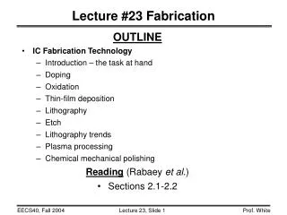
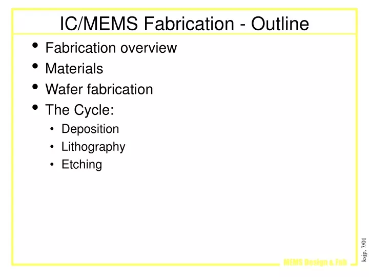
IC/MEMS Fabrication - Outline • Fabrication overview • Materials • Wafer fabrication • The Cycle: • Deposition • Lithography • Etching
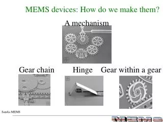
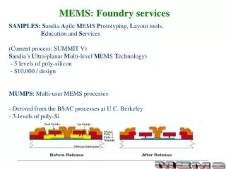
Fabrication • IC Fabrication • Deposition • Spin Casting • PVD – physical vapor deposition • CVD – chemical vapor deposition • Lithography • Removal • Wet etching • Plasma etching • Bulk Micromachining • Surface Micromachining • MUMPS • DRIE – deep reactive ion etch
Materials • Single crystal silicon – SCS • Anisotropic crystal • Semiconductor, great heat conductor • Polycrystalline silicon – polysilicon • Mostly isotropic material • Semiconductor • Silicon dioxide – SiO2 • Excellent thermal and electrical insulator • Thermal oxide, LTO, PSG: different names for different deposition conditions and methods • Silicon nitride – Si3N4 • Excellent electrical insulator • Aluminum – Al • Metal – excellent thermal and electrical conductor
Silicon properties • Semiconductor • Electrical conductivity varies over ~8 orders of magnitude depending on impurity concentration (from ppb to ~1%) • N-type and P-type dopants both give linear conduction, but from fundamentally different mechanisms • N-type touching P-type forms a diode • Cubic crystal • Diamond lattice • Anisotropic mechanical properties
Band Structure of Electron Energies • http://www.physics.udel.edu/wwwusers/watson/scen103/99s/clas0416.html • Bohr atom, Pauli exclusion principle • (not exactly right, but gives some intuition)
Doping semiconductors • Two different types of conduction • Electrons (negative, N-type) • Holes (positive, P-type) - - - - - - - - - - - - - o
V+ V- Tiny current ~pA N N P P Current exponentially dependent on voltage pA to kA in ~1V V- V+ Diodes
Silicon wafer fabrication • Taken from www.egg.or.jp/MSIL/english/index-e.html
Silicon wafer fabrication – slicing and polishing • Taken from www.egg.or.jp/MSIL/english/index-e.html
Wafers Deposition Lithography Etch Chips Process Flow • Integrated Circuits and MEMS identical • Process comlexity/yield related to # trips through central loop
Deposition Issues - Compatibility • Thermal compatibility • Thermal oxidation and LPCVD films are mutually compatible • Thermal oxidation and LPCVD are not compatible with polymers (melting/burning) and most metals (eutectic formation, diffusion, furnace contamination) • Topographic compatibilitiy • Can not spin-cast over large step heights • Distributed-source deposition over deep trenches leaves keyholes
Deposition Issues - Conformality • A conformal coating covers all surfaces to a uniform depth • A planarizing coating tends to reduce the vertical step height of the cross-section • A non-conformal coating deposits more on top surfaces than bottom and/or side surfaces Non-conformal Conformal Planarizing
An-isotropic Isotropic Etching Issues - Anisotropy • Isotropic etchants etch at the same rate in every direction mask
Mask target Etch stop Etching Issues - Selectivity • Selectivity is the ratio of the etch rate of the target material being etched to the etch rate of other materials • Chemical etches are generally more selective than plasma etches • Selectivity to masking material and to etch-stop is important
Spin Casting • Viscous liquid is poured on center of wafer • Wafer spins at 1000-5000 RPM for ~30s • Baked on hotplates 80-500C for 10-1000s • Application of etchants and solvents, rinsing • Deposition of polymers, sol-gel precursors
Physical Vapor Deposition - Evaporation • Evaporated metals in a tungsten crucible • Aluminum, gold • Evaporated metals and dielectrics by electron-beam • Refractory metals (e.g. tungsten) • Dielectrices (e.g. SiO2) • Typically line-of-sight deposition • Very high-vacuum required to prevent oxidation of e.g. aluminum
Physical Vapor Deposition - Sputtering • Sputtered metals and dielectrics • Argon plasma sputters material (small #s of atoms) off target • Ejected material takes ballistic path to wafers • Typically line-of-sight from a distributed source • Requires high vacuum depending on material
Thermal Oxidation Silicon is consumed as the silicon dioxide is grown. Growth occurs in oxygen and/or steam at 800-1200 C. ~2um films are maximum practical O2 SiO2 Silicon Silicon
SiO2 Thermal Oxidation • Oxidation can be masked with silicon nitride, which prevents O2 diffusion Silicon nitride Silicon
Chemical Vapor Deposition • Gases dissociate on surfaces at high temperature • Typically done at low pressure (LPCVD) rather than atmospheric (APCVD) • LPCVD pressures around 300mT (0.05% atmosphere) • Moderate Temperatures • 450 SiO2 • 580-650 polysilicon • 800 SixNy • Very dangerous gases • Silane: SiH4 • Arsine, phosphine, diborane: AsH3, PH3, B2H6
Wet etching • Extremely selective • Typically isotropic • Not widely used
Step coverage problems • Re-entrant sidewall angles cause discontinuity in metal lines
But isn’t perfect - Keyhole effect • Hemispherical/Isotropic deposition
Summary • Conformality of deposition is critical • LPCVD and thermal oxidation temperatures limit the materials that can be used • Selectivity of etchants is important • Anisotropy of etchants is important