Download
1 / 37
480 likes | 1k Views
IC/MEMS Fabrication - Outline. Fabrication overview Materials Wafer fabrication The Cycle: Deposition Lithography Etching. Fabrication. IC Fabrication Deposition Spin Casting PVD – physical vapor deposition CVD – chemical vapor deposition Lithography Removal Wet etching

E N D
IC/MEMS Fabrication - Outline • Fabrication overview • Materials • Wafer fabrication • The Cycle: • Deposition • Lithography • Etching
Fabrication • IC Fabrication • Deposition • Spin Casting • PVD – physical vapor deposition • CVD – chemical vapor deposition • Lithography • Removal • Wet etching • Plasma etching • Bulk Micromachining • Surface Micromachining • MUMPS • DRIE – deep reactive ion etch
Materials • Single crystal silicon – SCS • Anisotropic crystal • Semiconductor, great heat conductor • Polycrystalline silicon – polysilicon • Mostly isotropic material • Semiconductor • Silicon dioxide – SiO2 • Excellent thermal and electrical insulator • Thermal oxide, LTO, PSG: different names for different deposition conditions and methods • Silicon nitride – Si3N4 • Excellent electrical insulator • Aluminum – Al • Metal – excellent thermal and electrical conductor
Silicon properties • Semiconductor • Electrical conductivity varies over ~8 orders of magnitude depending on impurity concentration (from ppb to ~1%) • N-type and P-type dopants both give linear conduction, but from fundamentally different mechanisms • N-type touching P-type forms a diode • Cubic crystal • Diamond lattice • Anisotropic mechanical properties
Band Structure of Electron Energies • http://www.physics.udel.edu/wwwusers/watson/scen103/99s/clas0416.html • Bohr atom, Pauli exclusion principle • (not exactly right, but gives some intuition)
Doping semiconductors • Two different types of conduction • Electrons (negative, N-type) • Holes (positive, P-type) - - - - - - - - - - - - - o
V+ V- Tiny current ~pA N N P P Current exponentially dependent on voltage pA to kA in ~1V V- V+ Diodes
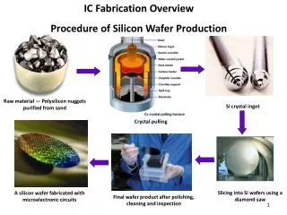
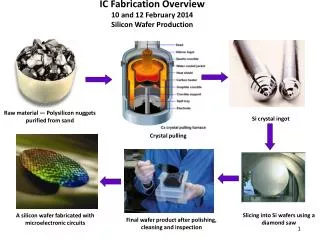
Silicon wafer fabrication • Taken from www.egg.or.jp/MSIL/english/index-e.html
Silicon wafer fabrication – slicing and polishing • Taken from www.egg.or.jp/MSIL/english/index-e.html
Wafers Deposition Lithography Etch Chips Process Flow • Integrated Circuits and MEMS identical • Process comlexity/yield related to # trips through central loop
Deposition Issues - Compatibility • Thermal compatibility • Thermal oxidation and LPCVD films are mutually compatible • Thermal oxidation and LPCVD are not compatible with polymers (melting/burning) and most metals (eutectic formation, diffusion, furnace contamination) • Topographic compatibilitiy • Can not spin-cast over large step heights • Distributed-source deposition over deep trenches leaves keyholes
Deposition Issues - Conformality • A conformal coating covers all surfaces to a uniform depth • A planarizing coating tends to reduce the vertical step height of the cross-section • A non-conformal coating deposits more on top surfaces than bottom and/or side surfaces Non-conformal Conformal Planarizing
An-isotropic Isotropic Etching Issues - Anisotropy • Isotropic etchants etch at the same rate in every direction mask
Mask target Etch stop Etching Issues - Selectivity • Selectivity is the ratio of the etch rate of the target material being etched to the etch rate of other materials • Chemical etches are generally more selective than plasma etches • Selectivity to masking material and to etch-stop is important
Spin Casting • Viscous liquid is poured on center of wafer • Wafer spins at 1000-5000 RPM for ~30s • Baked on hotplates 80-500C for 10-1000s • Application of etchants and solvents, rinsing • Deposition of polymers, sol-gel precursors
Physical Vapor Deposition - Evaporation • Evaporated metals in a tungsten crucible • Aluminum, gold • Evaporated metals and dielectrics by electron-beam • Refractory metals (e.g. tungsten) • Dielectrices (e.g. SiO2) • Typically line-of-sight deposition • Very high-vacuum required to prevent oxidation of e.g. aluminum
Physical Vapor Deposition - Sputtering • Sputtered metals and dielectrics • Argon plasma sputters material (small #s of atoms) off target • Ejected material takes ballistic path to wafers • Typically line-of-sight from a distributed source • Requires high vacuum depending on material
Thermal Oxidation Silicon is consumed as the silicon dioxide is grown. Growth occurs in oxygen and/or steam at 800-1200 C. ~2um films are maximum practical O2 SiO2 Silicon Silicon
SiO2 Thermal Oxidation • Oxidation can be masked with silicon nitride, which prevents O2 diffusion Silicon nitride Silicon
Chemical Vapor Deposition • Gases dissociate on surfaces at high temperature • Typically done at low pressure (LPCVD) rather than atmospheric (APCVD) • LPCVD pressures around 300mT (0.05% atmosphere) • Moderate Temperatures • 450 SiO2 • 580-650 polysilicon • 800 SixNy • Very dangerous gases • Silane: SiH4 • Arsine, phosphine, diborane: AsH3, PH3, B2H6
Wet etching • Extremely selective • Typically isotropic • Not widely used
Step coverage problems • Re-entrant sidewall angles cause discontinuity in metal lines
But isn’t perfect - Keyhole effect • Hemispherical/Isotropic deposition
Summary • Conformality of deposition is critical • LPCVD and thermal oxidation temperatures limit the materials that can be used • Selectivity of etchants is important • Anisotropy of etchants is important