Download
1 / 24
240 likes | 267 Views
Explore the development of detector electronics for cosmic radiation measurement, analyzing specifications, signal flow, noise management, and performance optimizations. This comprehensive guide covers design approaches, component details, and environmental robustness considerations in space applications.

E N D
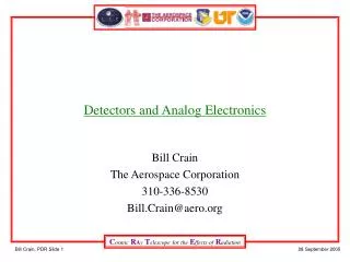
Detectors and Analog Electronics Bill Crain The Aerospace Corporation 310-336-8530 Bill.crain@aero.org
Introduction • Design Overview • Requirements Flowdown • Detector Specification • Signals, Noise, and Processing • Board Descriptions • Interface Block Diagram • Power Consumption • Trade Studies • Summary
Detector Electronics Design Overview • Detector electronics comprised of two board designs • Detector Boards in Telescope assembly • Analog Processing Board (APB) in E-box • Heritage approach from Polar CEPPAD/IPS unchanged from proposal • Linear pulse processing system utilizing Amptek hybrids • Circuits re-designed for CRaTER requirements • Functional requirements summary • Measure LET of high LET particles in thin detectors • Measure LET of low LET particles in thick detectors • Provide good resolution for TEP effects • No fast timing requirements • Robust to temperature drift and environments
Analog Signal Flow Diagram • Single fixed gain, linear transfer function • All detector channels use same topology • Differences in preamp input transistor, detector biasing, and gain settings are made to optimize thin and thick channels
Requirements Flowdown Electronics reqs. derived from Level 2 reqs. and detector sims.
Detector Specification (1) • Micron Semiconductor Limited • Lancing Sussex, UK • 20 years experience in supplying detectors for space physics • CEPPAD, CRRES, WIND, CLUSTER, ACE, IMAGE, STEREO, and more… • Detector Type • Ion-implanted doping to form P+ junction on N-type silicon • Very stable technology • Advantages to science include good carrier lifetime, stable to environmental conditions, and thin entrance windows
35 mm, diam. Guard P+ Contact Guard P+ window 0.1 um Active Volume (depletion region) 140 um thin; 1,000 um thick E-field N window 0.1 um N contact Detector Specification (2) • Circular detectors having active area of 9.6 cm2 • Two different detector thicknesses: thin and thick • note: state-of-the-art is 20um for thin and 2,000um for thick detectors • Guard ring on P-side to improve surface uniformity • Very thin dead layers (windows) reduce energy loss, lower series resistance, and reduce noise
Guard ring Al. contact plane Al. contact grid reduces surface resistivity Detector Specification (3) • Detector drawings (Micron)
Detector Specification (4) • ISO9001 • Full traceability and serialization • Travelers maintained • Verification and test prior to detector shipment • Random vibration test • Thermal cycling and thermal vacuum • Stability • Test criteria • Leakage current • I-V characteristic • Alpha resolution / pulser noise measurement (final test)
Nominal Threshold Nominal Threshold Proton Energy Deposition Simulations Reference: M. Looper GEANT4 Thin 150MeV incident E Thick 150MeV incident E Thin 1000MeV incident E Thick 1000MeV incident E
Iron Energy Deposition Simulation Reference: J.B. Blake
RFB CFB Ao Vpk = Qtot/CFB qμnNe(t)E qμpNh(t)E Cdet CFB (Ao) >> Cdet Signal Characteristics
Signal Processing (1) • Combined dynamic range of thin/thick pair is 5,000 • Thin threshold to provide overlap with thick range • Thin Detector Signal • Preamp input stage designed for 97% charge collection • High gain input jFET to raise dynamic input capacitance • 4% drift in operating point will result in 0.1% in output peak (< 1 bit) • Large feedback capacitance needed to handle Fe deposit • Preamp compensation to maintain closed-loop stability • Thick Detector Signal • Not as sensitive to detector capacitance • Design for low noise to maintain reliable 200 KeV low threshold and achieve < 1-bit resolution
+ input cap. T=peaking time F=shaping factors Noise Model (1) Reference: Helmuth Spieler IFCA Instrumentation Course Notes 2001
Optimum Noise Model (2)
Signal Processing (2) • Noise dominated by detector leakage and input jFET • Shaping time for both thin and thick detectors set at thick optimum point • ~1 usec • Compatible with A/D signal acquisition timing • 3-pole gaussian shaping improves symmetry and 2-complex poles shortens tail • Shaping reduces noise but also impacts signal level • S/N at thick detector threshold for this design ~ 4 • Translates to a noise occupancy in the coincidence window of < 0.1% for time period not greater than shaping time
Signal Processing (3) • Other factors affecting noise performance • Bias resistor sized to minimize voltage drop (i.e., maintain stable operating point) • Detector shot noise doubles every 8 C • Beneficial to operate cold; preferably below 20 C
Signal Processing (4) • Pileup is rare due to low event rate and relatively short shaping time • Exception: occasional periods of high ESP flux • Leading edge trigger technique causes timing uncertainty but coincidence window is large by comparison • Amplified low-level discriminator available to reduce walk • Ballistic deficit is not an issue due to short collection times relative to peaking time of shaper • Output voltage scaled for A/D input specifications
Detector Board • Thin/thick detector pair use same design topology • Signal collected on P-contact • Negative bias • Guard signal shunted to ground • No guard leakage noise • AC coupling to isolate DC detector leakage current • Low noise / high gain JFET input stage
Analog Processing Board • Single board in E-box contains 3 thin and 3 thick detector processing channels • Flight proven pulse processing components • Amptek A250 preamp hybrid utilizing external jFET on detector board • Shaping amps use Amptek A275 for active filtering • Baseline restorer, Amptek BLR1, compensates for baseline shifts on interface to A/D • Pole-zero cancellation circuit for correcting preamp pulse decay to eliminate undershoot • Test pulser injects ΔQ at preamp input jFET
Power Estimate Total estimated power dissipation is < 1 Watt
Trade Studies • Determine if one detector board can be implemented instead of three • Determine if A250 device should be located on detector board • Determine sensitivity of APB to detector performance • Want to avoid rework of APB when selecting/changing detectors during development • Determine how best to isolate chassis noise from detectors and preamp
Summary • Detectors are well-established technology from experienced supplier • Detector electronics design meets requirements of Level 2 mission and satisfies energy deposition levels determined by detector/TEP simulations • Trade studies in progress