Download
1 / 47
470 likes | 659 Views
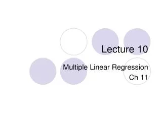
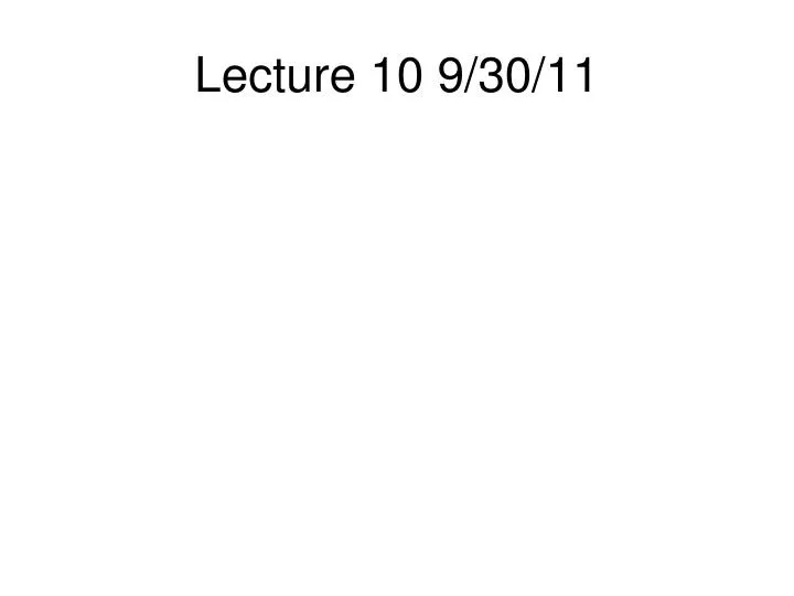
Lecture 10 9/30/11. Product Development Cycle. New Requirements. New Constraints. Specifications Constraints. Analyze the Problem. High-Level Design. Block Diagrams Data Flow Graphs. Engineering Design. Not Done. Testing. Implementation. Call graphs Data structures

E N D
Product Development Cycle New Requirements New Constraints Specifications Constraints Analyze the Problem High-Level Design Block Diagrams Data Flow Graphs Engineering Design Not Done Testing Implementation Call graphs Data structures I/O Interfaces Hardware Software Done! After Valvano, fig. 1.4
Stack use • With no OS, up to programmer to initialize SP, typically to high byte or word address in RAM • 6811: SP points to first free entry • 6812: SP points to last occupied entry • With MC68HC711E9, RAM runs $0000 to $01FF so you might expect LDS $01FF Some TExaS examples use this, but many TExaS examples use LDS $00FF presumably to support chips with only 256 bytes of RAM (though there are some with only 192 bytes…) NB if you are relying on Buffalo, it reserves $00-$FF for its own purposes, thus our ORG $0100 for RAM-based code/data; if BUFFALO is out of the loop, can ORG at $0000 • On MC68HC812A4, RAM $0800-$0BFF so appropriate statement is LDS $0C00
Purist stack use • Push, pulls only LDAA #1 PSHA LDAA #2 PSHA LDAA #3 PSHA • PULA: fully inherent: destroys top entry when restoring it to A. • We only ever access the top of the stack
Purist stack use • “Pure” use suffices for expression evaluation (as on RPN calculators) • But ECE152 should have taught you many other uses for stacks • return addresses • subroutine arguments • saved state • local variables • returned results • i.e. stack frames! • These can all require access to other than top entry of stack
Purist stack use • “Pure” use suffices for expression evaluation (as on RPN calculators) • But ECE152 should have taught you many other uses for stacks • return addresses • subroutine arguments • saved state • local variables • returned results • i.e. stack frames! • These can all require access to other than top entry of stack
Stack instructions PSHA PSHB PSHX PSHY PULA PULB PULX PULY DES decrement SP: SP = SP-1 (i.e. reserve space on stack) INS increment SP: SP = SP + 1 (i.e. discard top entry on stack)
Stack Frames To implement stack frames we will see we can use X and Y as frame pointers of a sort in chapter 8: TSX transfer S to X; 6811 does X = SP+1, 6812 does X=SP TSY TXS transfer X to S; 8611 does SP = X-1; 6812 does SP=X TXY We can do indexed addressing w.r.t. X or Y to get to contents of a stack frame; note 6811 allows only positive index offsets but 6812 allows positive and negative offsets.
Subroutines • Recall MIPS was bizarre • JAL/JR $RA was “half” a subroutine call/return • Motorola is conventional: BSR/JSR both call subroutine AND push return address on stack • BSR – relative addressing (8-bit 2’s comp displacement) • JSR – extended addressing (16-bit absolute)
Subroutines • BSR: 6 cycles • 2: read opcode/operand • 2: calc effective branch address • 2: store return address (2 1-byte xfers) • RTS: 5 cycles • 1: read opcode • 2: not sure! • 2: pop return address (2 1-byte xfers) • Stack discipline (frame pointers, etc) in later chapter
MC68HC11 Architecture • i.e. the packaged microcomputer, not the bare microprocessor • 4 operating modes • Single chip mode – our work so far – only resources used are those on the chip itself • Expanded mode – some extra memory and I/O devices are external to the chip (our boards can do this) • Bootstrap mode – can be used to IPL a program into RAM (IPL?) • Test mode – used by Motorola to verify correct operation of chip
68HC11: 9 major families • A,D,E,F,G,K,L,M,P • Decoding the parts • MC68JC11D0 is lowliest of the low, though some 6808/05 devices are lower! • Some have EEPROM – note EEPROM write times are about 10ms so not RAM substitute.
Ports - Directionality A: mix of in/out B: out only C:bidirectional D:bidirectional E: in only DDRC DDRD already encountered to control direction per pin
Opens up Pandora’s Box of control registers - All Memory Mapped
Details of 6811 Program Execution • Bus Interface Unit (BIU) reads from or writes to memory potentially each cycle • It must do something every cycle, if only killing time • With no pipelines, caches, speculative execution, branch history tables, etc. program timings are fully deterministic
7 variations on Read • All: R/W signal (explicit pin on chip)=1 and 16-bit effective address in EAR used to retrieve 8 bits of data • Instruction Fetch: EAR ← PC; IR ← [data]; • Page 2,3,4 accesses follow if 16-bit opcode but always start with 8 bits • Operand Fetch • Details vary with addressing mode, but operand is either directly (immediate) or indirectly (indexed, for example) embedded in instruction at location given by PC – get the part embedded in instruction itself (possibly followed by subsequent data fetch) • Opcode governs EAR generation and operand destination
7 variations on Read, cont. • Data Fetch: Address is EAR (computed with previously retrieved operand), 8-bit data go to register or directly to ALU • Stack Pull: SP ←SP+1; EAR ←SP; 8-bit data usually to a register • Three idle time killers: Freescale docs say which is used when • Null cycle: Address $FFFF, 8-bit data ignored • Dummy stack read: Address is SP, SP not changed, data ignored • Dummy PC read: Address is PC, PC not changed, data ignored
NB no DMA on 6811 • So CPU always in charge • R/W always 1 or 0, no “off” • newfound power awareness, would probably do things differently today!
2 kinds of write cycle • Data Write: 8 bit data from ALU or register stored at address given by EAR • Stack Write: 8-bit data from register stored at address given by SP, then SP ←SP-1 • Recall 6812 stack will be different!
6811 Instruction Cycle Details • Phase 1: Opcode Fetch • Each instruction has at least 1 byte of opcode • If first byte is $18, $1A, or $CD get second byte for page 2, 3, or 4 opcode • All RegY instructions have prebyte, making them longer/slower than RegX equivalents • Phase 2: Operand Fetch: varies with addressing mode • inherent: no operand • immediate: 1 or 2 byte operand, stored in register (ldaa #10) or directly to ALU (eora #$44)
6811 Instruction Cycle Details • Phase 2: Operand Fetch, cont. • direct (0-page): 1 byte of operand becomes EAR • extended: 2 byte operand becomes EAR • Indexed: 1 byte operand added to indexReg to form EAR • PC Relative: 1 byte operand added to PC to form EAR
6811 Instruction Cycle Details • Phase 3: Free cycles (Calc Address) • Before reading data (if required), EAR must be calculated – may require an “add” and thus must kill time • Indexed modes have 1 null cycle • Push/Pull have free cycles • Direct Page and Extended use EAR but don’t require null cycles (why!)
6811 Instruction Cycle Details • Phase 4: Data Read • If data needed from memory, EAR used to fetch 1 or 2 bytes (data fetches or stack pulls) • Phase 5: Free Cycles again (Execute) • Execute phase: bus is idle while ALU calculates something. Depending on instruction, one of the three cycle killing cycles are used while ALU is busy. • nb FDIV/IDIV take 41 cycles total, lots of free cycles!
6811 Instruction Cycle Details • Phase 6: Data Store • If memory write needed, write data to memory at EAR - 1 or 2 bytes depending on opcode. • Data writes or Stack pushes. • 6811 documentation gives cycle-by-cycle account of instructions
Older Motorola Doc notation (also used by TExaS) • f: free cycle (dummy fetch) • n: null cycle • x: dummy stack cycle • p: program byte access (both opcode and operand) • r: 8-bit data read • s: 8-bit stack data (i.e. push) • w: 8-bit data write • u: 8-bit unstack data (i.e. pull or pop) • v: vector fetch (later!) So an instruction might be described as (ppfrf) TExaS models 6811 cycle-by-cycle behavior accurately
6812 differences • In single chip mode, 6812 is also modeled correctly by TExaS • In expanded mode, possibility of cycle stretching exists (which Valvano doesn’t define!) • extra clock cycles inserted to allow access to slow external memory • 6812 can also do native 16 bit accesses or sequence of 8 bit accesses
6812 complications • Though cycle-accurate on 6811, some difficulties with TExaS on 6812:
6812 phases • Same as 6811 with addition of 16-bit reads and writes • No page 3,4 opcodes but more page 2 opcodes • Operand fetch can take up to 3 bytes for indexed modes • LDX $0800 with 6812 machine code $FE0800: real 6812 takes 3 16-bit memory cycles for this one: 1 for opcode, 1 for extended operand, 1 to read the 16-bit data: • TExaS will report as 5 1-byte transfers but report (correctly) they took 3 cycles to execute!
6812 Memory Interface • 6811 had only a R/W line, since all accesses were assumed to be 1 cycle and 8-bits • 6812 adds LSTRB signal, which when combined with knowing current address is even or odd permits 8/16 bit accesses as appropriate
Byte swapping? • Consider 16-bit (unaligned) read to 0x08FF: • LSB of word at 08FE is MSB but arrives as LSB; MSB of word at 0900 is LSB but arrives as MSB: processor swaps bytes. (double time penalty: 2 accesses plus swap) MSB LSB 08FE 0900
6812 Pipelining • 6812 uses idle bus cycles to fetch opcode and possibly operands of next instruction • details vary with 6812 model • NO overlapped execution: first instruction completes before second (potentially prefetched) instruction begins execution • pipeline is FIFO with 3 16-bit words • all reads hit the FIFO; writes bypass it • Real time course would obsess over timing details here!
6812 Pipelining • Whereas 6811 (short) branches take 3 cycles whether taken or not taken, pipeline and the associated FIFO mean short branches are described as “PPP/P” • i.e. 3 cycles if taken, 1 cycle if not taken, since in not taken case FIFO is already loaded with next instruction but in taken case FIFO needs to be reloaded.
MC68HC11 Port Replicator • Our “general purpose” ports each also have a special function • E: ADC – sensor interfaces • A: Timer subsystem – often critical in embedded systems to generate periodic signals • D: Built-in serial interface • Leaving only B,C • THESE disappear in expanded mode, becoming address/data bus for external memory
6824 Port Replicator, or “Peripheral Recovery Unit” • Added to expanded mode system, sits on A/D bus, re-creates Port B/C functionality Description The TK68HC24 is an exact replacement of the Motorola 68HC24. The TK68HC24 is designed to replace the Port B and Port C functions of 6811 – type microprocessors. These functions are lost when the 6811 type microprocessors are operated in the expanded mode. The TK68HC24 has an address re-mapping feature that allows multiple TK68HC24s to be used within a single system.
should be Port C
MC68HC12 Overview • Many more ports (12 vs 5) • Many more operating modes beyond single chip/extended • Additional addressing modes • which could be encountered on other embedded processors