Download
1 / 11
110 likes | 118 Views
This project explores the use of Monolithic Active Pixel Sensors (MAPS) as a potential replacement for diode pads in the Si-W ECAL for the ILC. MAPS integrate readout electronics onto the same wafer as the detecting element, allowing for a thinner design and increased density of pixels. This concept offers advantages such as improved energy measurement, finer granularity, and reduced cost.

E N D
MAPS for an ILC Si-W ECAL Paul Dauncey Imperial College London Paul Dauncey
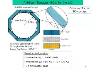
MAPS concept • Monolithic Active Pixel Sensors • Integrates readout electronics onto same wafer as sensitive detecting element • Uses standard CMOS technology, not high resistivity silicon as needed for Si-W ECAL with diode pads • Charge detection through ionisation in the epitaxial layer • Can be very thin; ~5-10mm and close to the surface; ~few mm • Charge diffuses within epitaxial layer to metal contact • Read out via electronics constructed on surface above this layer • Silicon wafers mechanically could be very similar to diode pads • Reuse almost all of diode pad mechanical structure ideas • “Simplest” approach would be to replace diode pad wafers with MAPS and integrate preamplifier (i.e. VFE ASIC circuit) into MAPS • But this does not take full advantage of the new possibilities… Paul Dauncey
MAPS concept • Readout concept is to go to a “digital” ECAL • Cover silicon in small pixels rather than diode pads • Use binary readout to keep data volume down • “Small” means probability of more than one track per pixel is low • Density of EM shower @ 500 GeV ~100 MIPs/mm2 in the core • Pixels have to be at most 100100 mm2 and probably more like 5050 mm2 • Results in 40k pixels instead of each diode pad • Gives ~107 pixels/wafer and ~1012 pixels in total for the ECAL! • Only vaguely feasible because of highly integrated electronics Paul Dauncey
Comparison of MAPS with diode pads • The PCB for both looks similar • But no VFE ASICs for MAPS case • Wafer thickness can be reduced • Only epitaxial layer detects charge • Don’t need full silicon thickness to get sufficient signal • This changes the thickness of the total slab structure by ~2mm • Still smaller even if MAPS mounted double-sided on PCB Paul Dauncey
Two options • Option 1: sum number of bits set over “pseudo-pad” • Area could be similar to original diode pad • Will give similar granularity • Difference is measurement is of number of particles, not deposited energy • Pixels act as “PDC” – Particle to Digital Converter! • Data rate per PCB ~3 Mbytes per bunch train • Interesting to know if sum area could be configurable or even event-by-event adaptive, depending on density of hits • Option 2: read beam crossing timestamps indicating when bits set for every pixel • More ambitious; total possible information • Clearly more flexible; option 1 is calculable from the data read out • Gives extremely fine granularity for pattern recognition • Downside is data rate; factor of ~3 higher • This is probably the favoured option at present Paul Dauncey
Advantages compared with diode pads • Energy measurement may be better • Pixels will measure the number of particles • Diodes measure the energy deposited in the silicon; depends on b and angle • David Ward’s studies show ~10-20% improvement in resolution at lowish energies • Granularity may be better (for option 2) • Two orders of magnitude improvement • Unclear how much is gained in actual PFLOW pattern recognition • Effective Moliere radius may be smaller • No VFE ASIC means wafer PCBs are thinner by ~1mm per layer • Reduces inter-tungsten gap; again how significant for physics? • Temperature stability may be better • Heat produced over whole wafer, not localised on VFE ASIC • Can use tungsten sheet as heat reservoir; bigger area for thermal coupling Paul Dauncey
Advantages (cont) • Assembly may be easier • Single-sided PCB and no VFE ASIC • Bump-bonding (standard commercial process), not gluing for wafers • Reduces assembly steps; there will be ~5k PCBs in the ECAL! • “Single event” upset may be reduced • Ionising particles can cause circuits to give corrupted results • Electronics will be hit by EM showers in both types of ECAL • Showers of order the Moliere radius ~9mm ~size of VFE ASIC so can affect whole chip • MAPS has much lower density of critical components • COST!!! • Currently standard CMOS more than a factor two cheaper than high resistivity silicon Paul Dauncey
What we will bid for • Three year programme to validate (or dismiss!) concept • Produce some prototype MAPS and test whether they work, in terms of signal size, noise rate, stability of threshold/pedestal, etc. • Ideally, put in a beam test for further checks, including single event upsets • Plan for two iterations of wafer manufacturing • These would be produced around 18 and 30 months into project • First iteration will have several different designs • Around nine, each on a ~11 cm2 (or smaller) area • Test various choices for comparator, readout, reset, etc. • Second iteration will be a single design • Use modification of the best design from first iteration • Make 22 cm2 area devices; standard commercial size • Would get standard run of six wafers, each holding ~ 50 sensors • Even allowing for bad yield, would be able to make several layers of e.g. 1010 cm2 area for a beam test Paul Dauncey
Simulation work is needed! • Many of the arguments need firming up before proposal goes in • Need quantitative answers to many questions • First thing is to write a realistic simulation of a MAPS including the thin sensitive layer • What pixel size is really needed? • Is 5050 mm2 sufficient? • Would we see saturation effects from multiple tracks per pixel? • What is the requirement on noise in the pixels? • How often can we tolerate a fake hit in a pixel? • Signal/noise of >10 could give 10–6 probability of fake hit, if Gaussian • Is one fake in every 106 samples good enough for physics? • This impacts both resolution on the shower energy and pattern recognition; which is the more critical? Paul Dauncey
Simulation work (cont) • What is the actual improvement in using pixels not diode pads? • Preliminary studies on energy resolution started • Does the answer depend on the option chosen? • What about pattern recognition? • What is a tolerable inefficiency per pixel? • The surface readout electronics may absorb some charge • May be a localised inefficiency; is this acceptable? • Does it affect resolution or pattern recognition more? • What rate of crosstalk is acceptable? • Diffusion means tracks near pixel edges will share charge with neighbour • Better to have low threshold and hence two hits, or high threshold and hence zero hits? • What rate of sharing is tolerable? Paul Dauncey
Simulation work (cont) • What is the rate from beam interactions in the pixels? • If too high, then the data volume would be prohibitive • TESLA TDR gives a rate of around each diode pad being above threshold once per train • How does this translate into pixels per train; 10 per diode? 100? 1000? • What would be the difference in temperature stability? • Need thermal modeling rather than GEANT • Could make a difference between requiring cooling pipes or not? • What improvement is achieved with a 1mm gap reduction? • Is this significant for shower separation? Two months to answer as many of these questions as we can • Please contact me if you want to help out here! Paul Dauncey