Download
1 / 26
270 likes | 581 Views
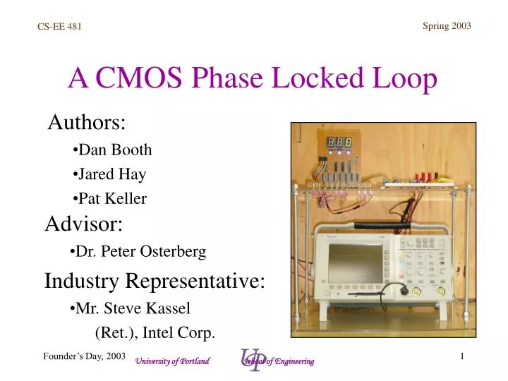
A CMOS Phase Locked Loop. Authors: Dan Booth Jared Hay Pat Keller. Advisor: Dr. Peter Osterberg Industry Representative: Mr. Steve Kassel (Ret.), Intel Corp. Agenda. Introduction Dan Booth Background Dan Booth Methods Pat Keller Results Pat Keller Conclusions Jared Hay

E N D
A CMOS Phase Locked Loop Authors: Dan Booth Jared Hay Pat Keller • Advisor: • Dr. Peter Osterberg • Industry Representative: • Mr. Steve Kassel • (Ret.), Intel Corp. University of Portland School of Engineering
Agenda • Introduction Dan Booth • Background Dan Booth • Methods Pat Keller • Results Pat Keller • Conclusions Jared Hay • Demonstration Jared Hay University of Portland School of Engineering
Special Thanks Dr. Peter Osterberg Mr. Steve Kassel Dr. Wayne Lu Ms. Sandra Ressel MOSIS Educational Program Introduction University of Portland School of Engineering
Introduction • Project problem definition: • Synthesize 90-110kHz from a 1kHz reference • Why frequency synthesis? • Frequency generator • Signal conditioning • Clock multiplication University of Portland School of Engineering
Introduction • Goals • Understanding of our Phase Locked Loop: • Architecture • Operation • Applications University of Portland School of Engineering
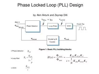
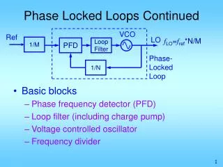
fout fin VC Verror Phase frequency detector Loop filter VCO fd Frequency Divider CMOS Chip N Control Background • Phase Locked Loop Architecture University of Portland School of Engineering
Background • What our PLL frequency synthesizer does: • Produces an output of 90-110kHz in 1kHz increments • fin = 1kHz • N = integers from 90 to 110 • fout = N*fin = 90 – 110kHz • Key functional specifications: • fin and fout are 0 to 5 volt digital signals • Lock range of 90 – 110kHz University of Portland School of Engineering
fin fin fin fd fd fd verror verror verror fd fd Background Phase Lock Feedback Situation A: Frequencies are in phase - VC held constant Situation B: fin leads fd - VC increases Situation C: fd leads fin - VC decreases University of Portland School of Engineering
Methods Phase I: Research of PLLs University of Portland School of Engineering
Methods Phase II: Design of Chip • B2Logic Simulations- Phase Frequency Detector- Frequency Divider • Custom Design! • TPR File- CMOS Chip Layout University of Portland School of Engineering
Methods Phase III: Building • Macromodel of Chip • VCO configuration- set control voltage range, VC- set output frequency range • Loop Filter- 2nd order low pass filter- set pole and zero for stability University of Portland School of Engineering
Methods • Closing the feedback loop- Achieving lock • User interface- N-Control switches- Seven-segment displays University of Portland School of Engineering
Digital CMOS Chip Frequency Divider Phase Frequency Detector Results = University of Portland School of Engineering
Results • Off Chip Components • Loop Filter • Voltage Controlled Oscillator University of Portland School of Engineering
Conclusions • CMOS Chip works! • Operation is stable • Increased Performance • Output range: 51 – 127kHz • Limited by VC range of 0-5 V University of Portland School of Engineering
Conclusions • Possible Improvements • Increase reference frequency accuracy • Crystal oscillator • Applications • Frequency generator • Signal conditioning • Clock multiplication University of Portland School of Engineering
Demonstration • Power up • fout displayed on scope- fout is N times fin - Lock is achieved quickly University of Portland School of Engineering
Questions? University of Portland School of Engineering