Download
1 / 40
500 likes | 997 Views
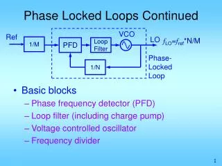
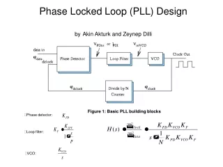
CSE598A/EE597G Spring 2006. Phase Locked Loop Design. KyoungTae Kang, Kyusun Choi Electrical Engineering Computer Science and Engineering. Frequency Synthesizer. General Synthesizer Issues. Frequency Spectrum. Settling Time (Lock Time). PLL Components Circuits. PLL Components Circuits.

E N D
CSE598A/EE597G Spring 2006 Phase Locked Loop Design KyoungTae Kang, Kyusun Choi Electrical Engineering Computer Science and Engineering
PFD and Charge Pump Spur!!
PFD and modified flip-flop B.park, “A 1GHz, Low-Phase-Noise CMOS Frequency Synthesizer with Integrate LC VCO for Wireless Communications“, CICC 1998 Park, Byungha? GIT PhD. Samsung LSI, RF/Analog IC Group
New Modified flip-flop by KT • Reduce signal path • High speed • 10 Transistors • Negative reset • No oscillation • Customized
DFF Simulation Comparison • Modifed FF by KT • DFF
PFD Output Stage-Charge Pump Programmable
Charge Pump (Drain–s/w) • My first Charge pump. • Easy to design and understand how to work • Spike Noise from net76 when U2 turn on • High noise contribution! • If you designed CP like this, you got fired!
Charge Pump (Source-s/w) • Low charge sharing • Low noise • Suppression the Spur Why? Cascode? >High impedence >Pole!!! Level?
Charge Pump Simulation CP_Drain CP_Source V(U/D) I(U) I(D)
Rhee, W., "Design of high performance CMOS charge pumps in phase locked loop", In Proc. ISCAS, 1999, Vol. 1, pp. 545-548 J. S. Lee, M. S. Keel, S. I. Lim, and S. Kim, “Charge pump with perfect current matching characteristics in phase-locked loops,”Electronics Letters, Vol. 36, No. 23, pp. 1907-1908, November 2000. Charge Pumps
Differential Delay Cell-Single pass Chan-Hong Park, Solid-State Circuits, 1999.
Differential Delay Cell-Multiple pass Negative Skewed Delay Scheme: Seog-Jun, Lee, ISSC, 1997 Yalcin Alper Eken, Solid-State Circuits, 2004
Multiple pass Ring OSC. • Which one is faster? • 3 stage single pass Ring OSC. • 5 stage multiple pass Ring OSC.
3 Stage-Single pass Ring OSC. • 220MHz~825MHz @ V(Ctrl)=1.65V~3.3V
5 Stage-Multiple pass Ring OSC. • 1.65GHz~2.5GHz @ V(Ctrl) 1.65V~3.3V
.Option Transient Step Start-up time Triggered Signal Frequency Measure Tool: Cscope How to simulate Oscillator in Hspice?
Frequency Divider • Input stage-high speed, low power, Following stages-High speed • Differential type-Suppression Noise • Input buffer is required
PLL Simulation V(VCO) V(Ref) V(DiV) V(Up) V(Dn) V(Ctrl)