Download
1 / 14
160 likes | 499 Views
A Fast-Locked All-Digital Phase-Locked Loop for Dynamic Frequency Scaling. Dian Huang Ying Qiao. Motivation. CMOS IC technology keeps further scaling SoC benefits from All-Digital PLL (ADPLL) designs Dynamic frequency scaling in CPU Fast-locked phase-locked loop (PLL) for clock generation

E N D
A Fast-Locked All-Digital Phase-Locked Loop for Dynamic Frequency Scaling Dian Huang Ying Qiao
Motivation • CMOS IC technology keeps further scaling • SoC benefits from All-Digital PLL (ADPLL) designs • Dynamic frequency scaling in CPU • Fast-locked phase-locked loop (PLL) for clock generation • Tradeoffs between locking time and clock jitter • We will focus on • ADPLL design with bang-bang phase detector (BBPHD) • Digitally controlled oscillator (DCO) frequency-search using algorithms with Successive-Approximation Registers (SAR)
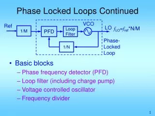
ADPLL Architecture • Conventional vs. Proposed ADPLL Architecture Conventional BBPHD ADPLL Proposed BBPHD ADPLL with SAR
Design Considerations • Tradeoff exists between frequencyphase locking time and output clock jitter performance – reference clock frequency – initial frequency error – system loop gain β - Proportional path gain α – Integral path gain
Fast-locking Techniques • Simultaneous frequency and phase locking • Yang, JSSC ’10 – adaptive loop gain • Hung, Trans Circuit & Syst. ’11 – modified bang-bang algorithm • Detangled frequency and phase locking • Chung, JSSC ’11 – BSA frequency search + TDC phase locking
SAR-based Frequency Search Reference clock Divider output Oscillator output BBPHD UP signal
SAR-based Delay Search • Falling edge of divider output does not align with that of reference clock due to delay. • Add extra delay to reference clock • Once frequency search is done, CPU designer can choose whether input clock of PLL is reference clock or its delay version based on jitter and locking requirement.
Locking Procedure • 2 cycles delay-search, 10 cycles frequency-search for a 10 bit DCO. • Remained frequency error and phase error are tiny. • Locks at 790ns
Five Stage DCO • DCO consists of 960 tri-state buffer: 64 row with each row has 15 buffers. • Five extra tri-state buffer are used to drive each to node to either Vdd or ground during reset for fast start-up • DCO Frequency Range: 0.42GHz ~ 12GHz
PI Controller • With proposed frequency-search algorithm, small and can be chosen. • needs to be several time larger than for stability, but want to be 1 or 2 to minimize the quantization noise. • Integral path code increment by 1 only when it can increment by 4
Performance • Achieves 790ns locking time while maintaining 1.32ps rms jitter. • Peak-to-peak jitter is too optimistic.
Conclusion • Proposed ADPLL realizes fast-locking without sacrificing jitter performance. • 790ns locking time demonstrates that it is suitable to dynamic frequency scaling. • Future work includes ADPLL with smooth frequency change so that CPU does not needs to stall its instructions.